


sales@plutosemitech.com | WhatsApp:  +86-17701852595

Our Story

Plutosemi Co., Ltd

Founded in 2019 and based in Foshan Nanhai, Plutosemi Co., Ltd. specializes in high-performance semiconductor materials. As an industry leader, we offer advanced production capabilities and high-quality products such as silicon wafers and SOI, featuring high precision for diverse applications. Our one-stop services and customized solutions meet specific customer needs. Widely used in China, Europe, and the USA, we maintain strong partnerships with renowned international companies, upholding the philosophy of "Customer First, Quality Foremost".

Learn More

Product Center

Glass Wafer

Learn More

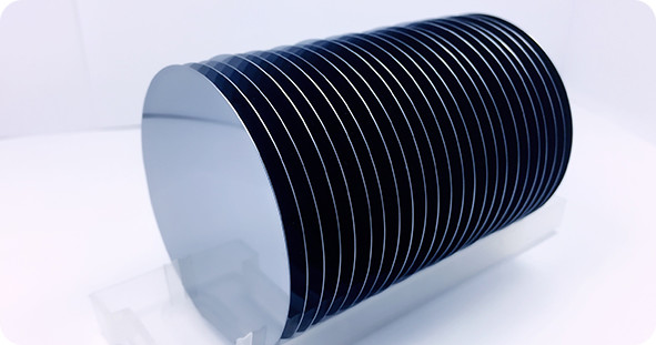
Silicon Wafer

Learn More
Silicon Wafer

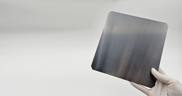
Solar Wafers

Learn More
Solar Wafers
Learn More

Exhibition

Innovation

PLUTOSEMI-Innovation

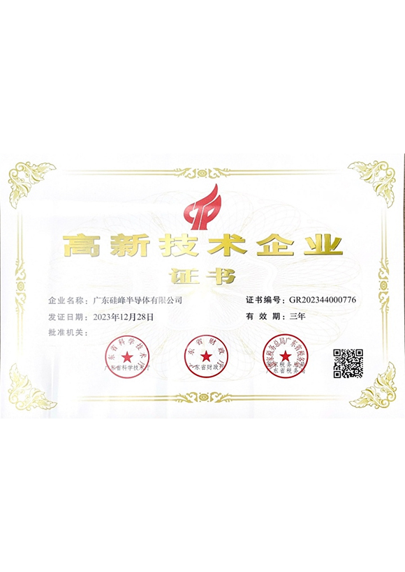
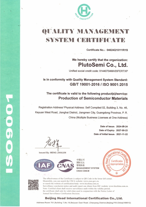
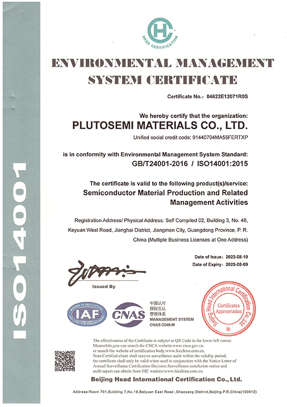
Certificate

The company maintains industry-leading standards with certifications in high-performance semiconductor materials R&D, production, and sales, supporting its position as a leader in the semiconductor materials sector.

How Does Glass Thermal Expansion Affect Wafers?

Temperature changes are unavoidable during semiconductor processing, bonding, coating, and packaging. When glass wafers experience heating or cooling, their dimensions change according to their thermal expansion characteristics. The glass wafer thermal properties directly influence process compatibility, especially when wafers are combined with silicon, metals, polymers, or other materials.

How Are Sapphire Substrates Tested?

Sapphire substrates are widely used in semiconductor, optical, and electronic applications because of their high hardness, thermal stability, and excellent optical properties. However, the performance of a sapphire substrate depends strongly on crystal quality, surface condition, dimensional accuracy, and internal defect control.

How Are Semiconductor Wafers Inspected?

Semiconductor wafers require strict inspection before entering device fabrication because even microscopic defects can influence production yield, electrical performance, and process stability. Modern semiconductor manufacturing involves dozens of precision steps, including lithography, deposition, etching, implantation, and packaging.

Home

Products

Phone

About

Inquiry