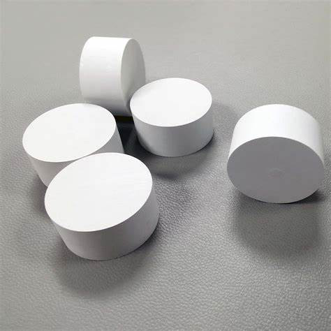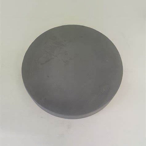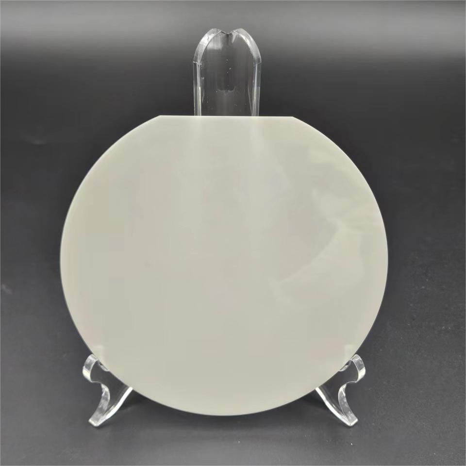
Gray Aluminum Nitride Wafer
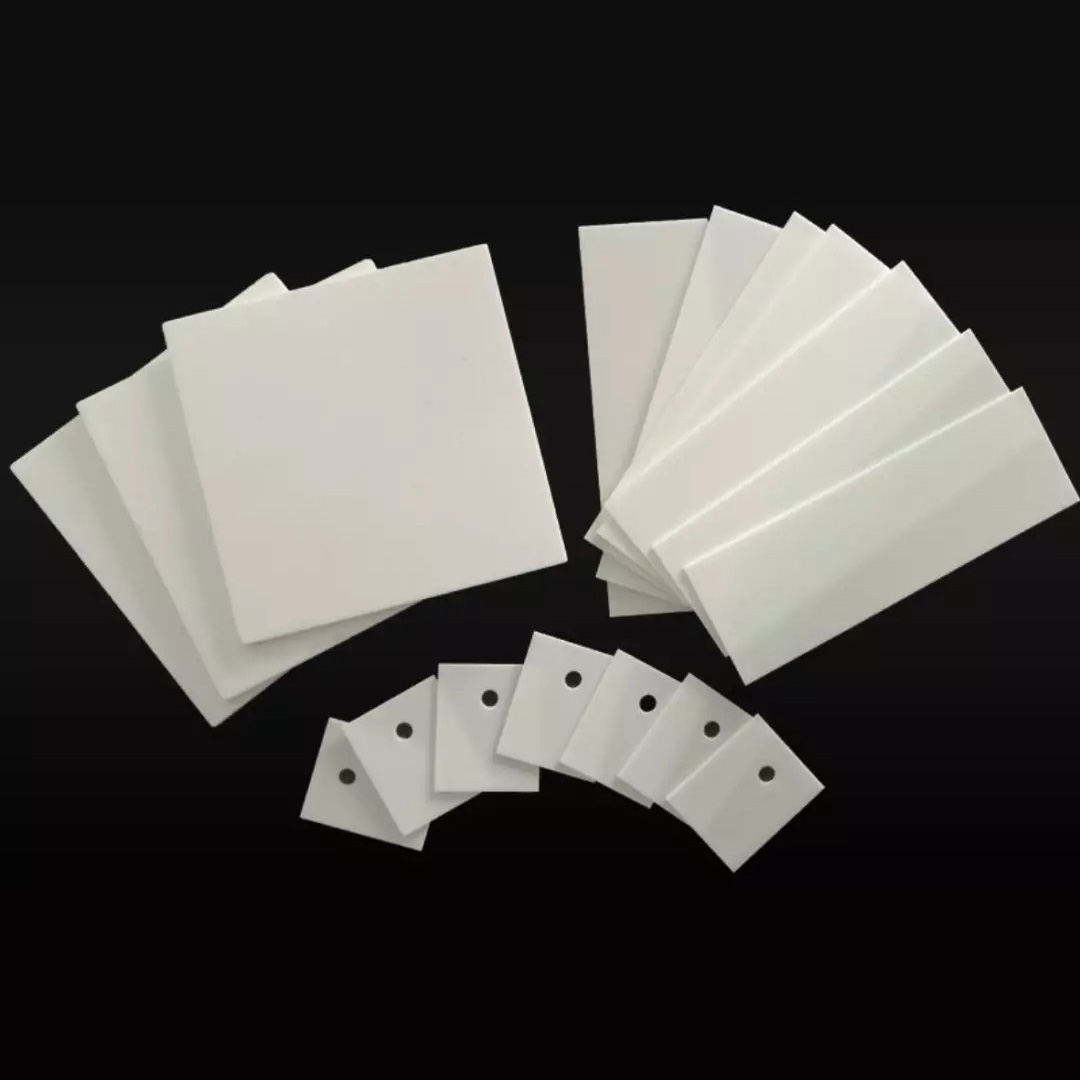
Ceramic Wafers

-
+86-17701852595 WhatsApp
-
sales@plutosemitech.com Email
Aluminum Nitride Wafer is a high-performance ceramic material wafer that has emerged in the semiconductor industry, electronic packaging, and many high-tech fields due to its unique physical and chemical properties. Its wafer form is refined through advanced powder metallurgy and ceramic processing technology, refining aluminum nitride powder through complex processes such as molding and sintering, presenting a gray or gray black color, smooth surface, and precise size.

Gray Aluminum Nitride Wafer Specifications
Product Standard:
| Product Name | Color/Purity/Method | Size | Thickness | Thickness |
| AlN ceramic substrate | Gray | 114.3 x 114.3mm 101.6 x 101.6mm 100 x 100mm 76.2 x 76.2mm 50 x 50mm 10 x 10mm φ50.8mm φ100mm Or others | 0.1mm 0.25mm 0.385mm 0.5mm 0.635mm 1.0mm 2.0mm Or others | Un-polished surface Single side polished Double side polished Unpolished: Ra 0.2~0.75um Polished: Ra 0.02~0.05um Best Polished: Ra < 10nm |
Product Specifications:
| Product Name | Aluminum Nitride(AlN) ceramic plate/substrate |
| Material | Aluminum Nitride(AlN) |
| Density (g/cm3) | > 3.33 |
| Water Absorption | 0% |
| Color | Gray |
| Dielectric Constant | 8~10 (1MHz) |
| Flexural Strength | > 450 Mpa |
| Dielectric Strength | > 17 KV/mm |
| Volume resistivity (20°C) | > 10E13 ohm-cm |
| Thermal Conductivity (20°C) | > 170 W/(m.K) |
| Thermal Expansion Coefficient (10-6/°C) | 2~3(20~300°C) 2.5~3.5 (300~800°C) |
Gray Aluminum Nitride Wafer Features
1. High thermal conductivity:
Aluminum nitride wafers have extremely high thermal conductivity, far exceeding traditional ceramic materials and even approaching certain metal materials. This characteristic makes aluminum nitride wafers perform well in electronic devices that require efficient heat dissipation, such as LED lighting, power semiconductor modules, etc., which can effectively reduce the operating temperature of the device, improve stability and lifespan.
2. Good electrical insulation:
Aluminum nitride wafers are excellent electrical insulators with extremely high resistivity, which can effectively isolate electronic signals, prevent current leakage or short circuits, and ensure the normal operation of electronic devices.
3. Excellent mechanical strength:
Aluminum nitride wafers have high strength and hardness, can withstand significant mechanical stress and impact, are not easily deformed or broken, and provide solid physical support for electronic devices.
4. Excellent chemical stability:
Aluminum nitride wafers have good resistance to most chemical reagents, are not prone to chemical reactions or corrosion, and can maintain stable performance in harsh environments.
5. Precise dimensional control:
Through advanced processing techniques, aluminum nitride wafers can achieve high-precision size control, meet the demand for precision components in modern electronic devices, and improve product reliability and consistency.
Gray Aluminum Nitride Wafer Application
1. High frequency electronic devices: In high-frequency applications such as 5G communication and radar systems, Aluminum Nitride Wafer is used to manufacture high-frequency circuits and devices, which can effectively process high-power signals and improve equipment performance.
2. Optoelectronic devices: Due to their excellent optical properties, this wafer is widely used to manufacture optoelectronic devices such as LEDs and lasers, and can operate in a wide wavelength range from ultraviolet to mid infrared.
3. Automotive electronics: in electric vehicles and autonomous vehicle, it is used to manufacture power devices and sensors, which can withstand high temperature and humidity environments, and improve the safety and reliability of vehicles.
4. Medical field: In fields such as medical imaging and disease diagnosis, this type of wafer is used to manufacture devices such as ultrasonic sensors, which can provide high-resolution images and accurate diagnostic information.
5. Aerospace: Gray Aluminum Nitride Wafer is used in the aerospace industry, such as satellite communication and avionics systems, to manufacture electronic components that are resistant to radiation and high temperature environments, ensuring that equipment operates normally under extreme conditions.
Plutosemi Co., Ltd. was established in 2019, headquartered in Nanhai, Foshan, focusing on the research and development, production, and sales of high-performance semiconductor materials.
Advanced production capacity: We have three major production bases in China, with a monthly production capacity of 100000 equivalent 6-inch silicon wafers and 30000 equivalent 8-inch glass wafers, ensuring stable and efficient product supply for our customers.
High quality products: We provide efficient and stable product supply innovative solutions in the fields of glass wafers, silicon polishing wafers, epitaxial wafers (EPI), silicon on insulator wafers (SOI), and more. Our silicon wafers have the characteristics of ultra-thin, ultraflat, and high-precision, which can meet the needs of various high-end applications. Our glass and quartz substrates are also renowned for their high smoothness and precise aperture design.