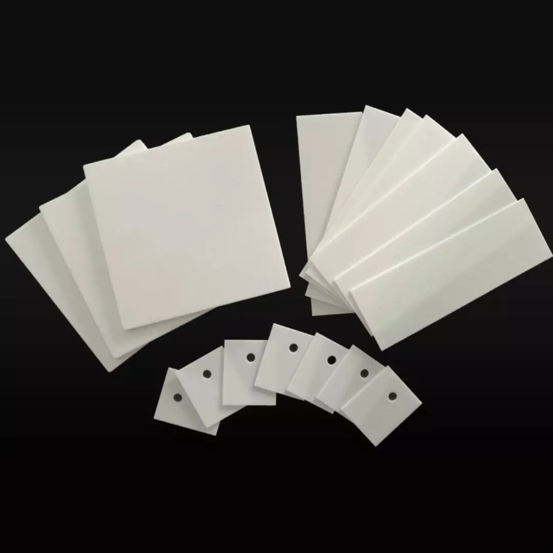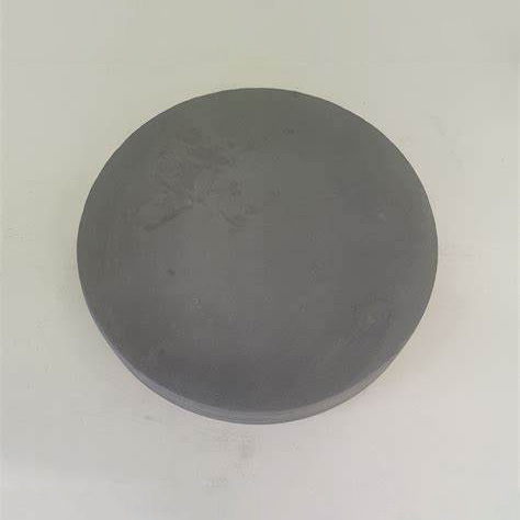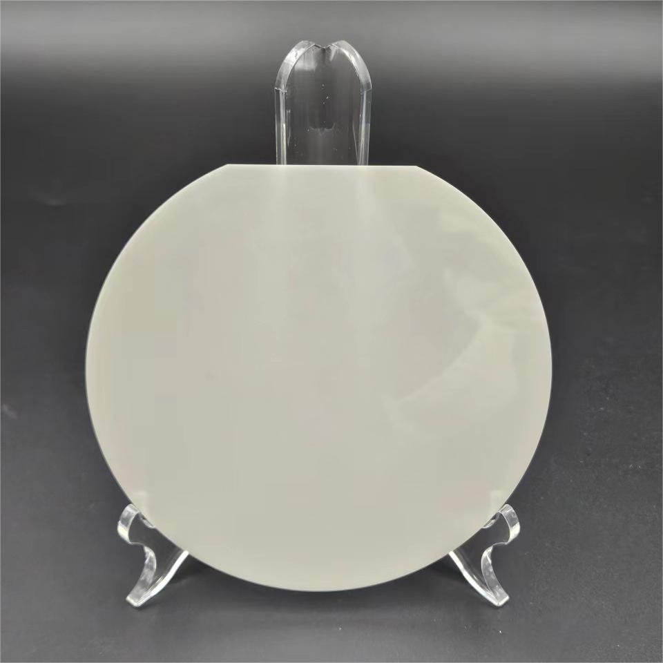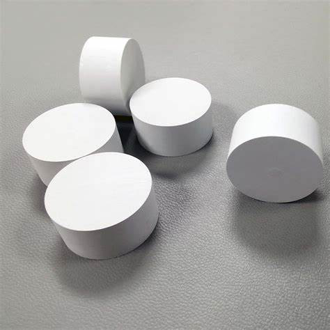
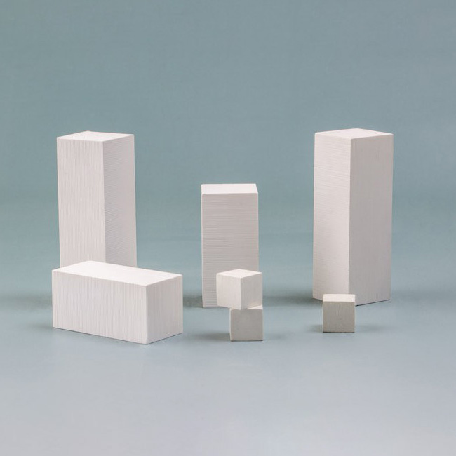
Heat Resistance Boron Nitride Wafer
Ceramic Wafers

-
+86-17701852595 WhatsApp
-
sales@plutosemitech.com Email
Boron nitride wafer is mainly composed of boron nitride (BN) and processed through advanced manufacturing processes, possessing stable physical and chemical properties. Boron nitride silicon, as an advanced ceramic material, has shown wide application prospects in various fields such as semiconductors, electronics, optoelectronics, and new energy due to its unique layered structure and excellent thermal conductivity. This wafer not only inherits all the advantages of boron nitride silicon material, but also has been comprehensively optimized in terms of heat resistance, mechanical strength, chemical stability, etc. It is an ideal choice to meet the demand for high-performance materials in modern high-tech industries.

Heat Resistance Boron Nitride Wafer Specifications
| Item | Unit | SiC |
| Purity | % | 99 |
| Density | g/cm3 | 2 |
| HV Hardness | Gpa | 3 |
| Thermal Conductivity | W/m·K | 30 |
| Coefficient of Thermal Expansion (CTE) | 1E-6/℃ | 2 |
| Modulus of Elasticity | GPa | 60 |
| Compressive Strength | MPa | 160 |
| Bending Strength | MPa | 80 |
| Thermal Shock | ℃ | / |
| Breakdown Voltage | KV/mm | 3 |
| Dielectric Constant | / | 4 |
| Maximum Operating Temperature | ℃ | 2200 |
Heat Resistance Boron Nitride Wafer Features
1. High thermal stability:
The Heat Resistance Boron Nitride Wafer is able to maintain stability at extremely high temperatures, thanks to its unique hexagonal boron nitride structure. This structure endows it with the ability to withstand temperatures up to 2000 ℃ or even higher without structural damage or performance degradation. This excellent high thermal stability makes it an indispensable material in many high-temperature application scenarios.
2. Good electrical insulation:
Boron Nitride Wafer has excellent electrical insulation performance and can effectively isolate current in high voltage and high current environments, protecting the stable operation of circuits. This is due to its wide bandgap characteristic, which allows it to withstand high-intensity electric fields without breakdown. Its insulation performance is not affected by environmental factors, and even under harsh conditions such as high temperature and high humidity, it can still maintain good insulation effect.
3. Excellent thermal conductivity:
It also has excellent thermal conductivity, which can quickly conduct and dissipate heat. The unique crystal structure of hexagonal boron nitride results in extremely high in-plane thermal conductivity, second only to diamond. Phonons experience minimal scattering and obstruction during propagation in crystals, effectively conducting heat.
4. Low thermal expansion coefficient:
The thermal expansion coefficient of Boron Nitride Wafer is very low, and there is almost no size change when the temperature changes. This is because the arrangement of boron and nitrogen atoms in its crystal structure is very compact and stable, resulting in minimal isotropic expansion of the material when heated. It can effectively prevent material cracking and damage caused by thermal stress.
5. Chemical stability:
It also has extremely high chemical stability and hardly reacts with the vast majority of chemical substances. Whether in corrosive environments such as strong acids and alkalis, or under extreme conditions such as high temperature and high pressure, it can maintain the stability of its chemical properties, ensuring the quality of the product and the safety of the production process.
Heat Resistance Boron Nitride Wafer Application
1. Thermal management of electronic devices:
Heat Resistance Boron Nitride Wafer is widely used as an efficient thermal management material. In chip packaging, it can serve as a heat dissipation substrate or thermal interface material, quickly conducting the heat generated by the chip to the heat sink or external environment, effectively reducing the operating temperature of the chip and improving the stability and service life of the device.
2. Aerospace high-temperature components:
In aircraft engines, it can be used as a coating or substrate material for high-temperature components such as turbine blades and combustion chambers. Its high thermal stability and low thermal expansion coefficient can effectively resist the erosion and thermal fatigue of high-temperature gas, extend the service life of components, and improve the performance and reliability of the engine.
3. High performance automotive components:
In the battery system of electric vehicles, it can serve as a heat dissipation material and insulation material for battery modules. Its thermal conductivity ensures that the heat generated by the battery during charging and discharging can be dissipated in a timely manner, preventing safety issues caused by battery overheating; At the same time, its good electrical insulation can effectively isolate the current between battery cells, improving the safety and stability of the battery system.
4. Energy storage field:
The boron nitride wafer also has broad application prospects in the field of energy storage. In lithium-ion batteries and solid-state batteries, it can serve as a carrier and separator material for electrode materials. Its high specific surface area and good thermal conductivity help improve the charging and discharging performance of batteries. In some new energy storage technologies, such as thermal energy storage and fuel cells, it is also used as a heat exchange material and catalyst carrier to provide support for efficient energy storage and conversion.
5. Manufacturing of optical components:
In some special optical instruments, such as space telescopes and high-precision spectrometers, it is used as the substrate material for lenses and reflectors. Its low thermal expansion coefficient and high dimensional accuracy can effectively maintain the stability of the optical system, improve the measurement accuracy and performance of the instrument. In laser processing equipment, it can serve as a window material for laser transmission, ensuring stable transmission of the laser beam and normal operation of the equipment.

Plutosemi Co., Ltd. was established in 2019, headquartered in Nanhai, Foshan, focusing on the research and development, production, and sales of high-performance semiconductor materials.
Advanced production capacity: We have three major production bases in China, with a monthly production capacity of 100000 equivalent 6-inch silicon wafers and 30000 equivalent 8-inch glass wafers, ensuring stable and efficient product supply for our customers.
High quality products: We provide efficient and stable product supply innovative solutions in the fields of glass wafers, silicon polishing wafers, epitaxial wafers (EPI), silicon on insulator wafers (SOI), and more. Our silicon wafers have the characteristics of ultra-thin, ultraflat, and high-precision, which can meet the needs of various high-end applications. Our glass and quartz substrates are also renowned for their high smoothness and precise aperture design.