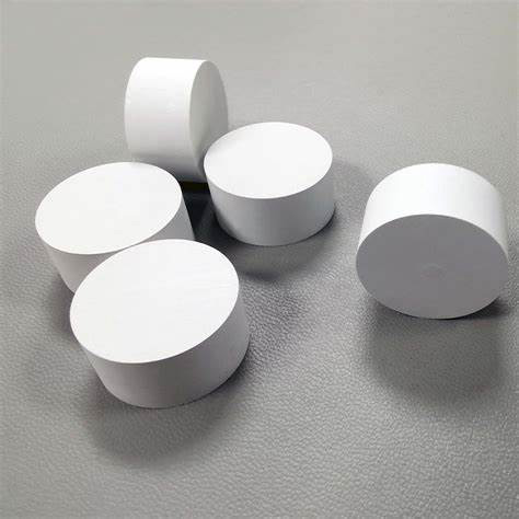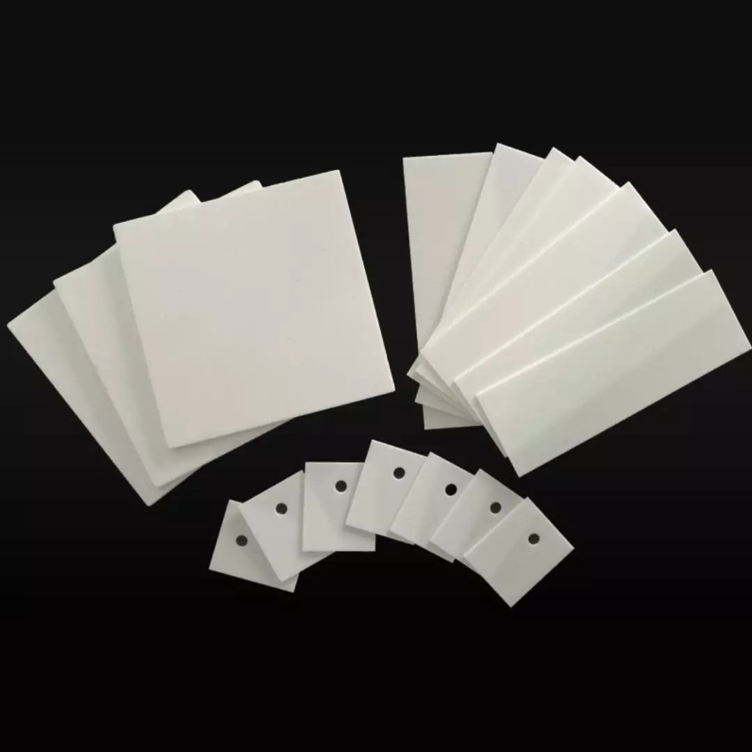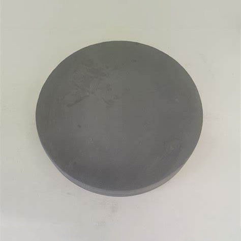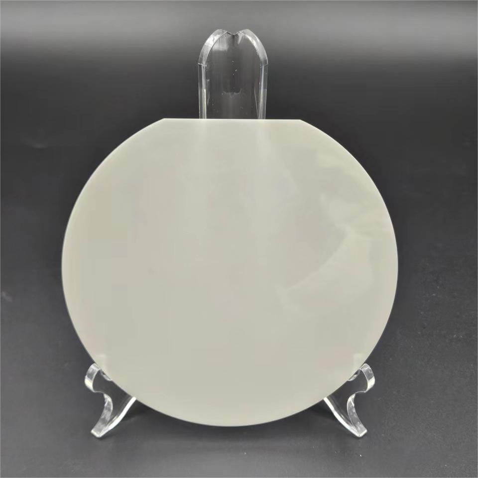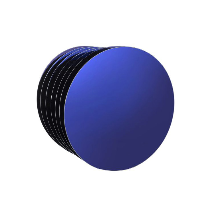
High Precision Silicon Nitride Wafer
Ceramic Wafers

-
+86-17701852595 WhatsApp
-
sales@plutosemitech.com Email
The strength of High Precision Silicon Nitride Wafer is very high, especially hot pressed Silicon nitride, which is one of the hardest substances in the world. It is extremely resistant to high temperatures, its strength can be maintained to a high temperature of 1200 °C without falling, it will not melt into a melt after heating, it will decompose until 1900 °C, and silicon nitride wafer has amazing chemical resistance and can withstand almost all inorganic acids?and less than 30% caustic soda solution. It can also withstand the corrosion of many organic acids; it is also a high-performance electrical insulation material. Silicon nitride ceramics can be used as gas turbine combustion chambers, mechanical seal rings, the pipes and valves for electromagnetic pumps that transport aluminum liquid, permanent molds, and steel water separation rings. As a professional China silicon nitride wafer manufacturer, we specialize in delivering high-performance Si3N4 wafers for advanced industrial and technological applications.

Product Standard:
| Product Name | Color/Purity/Method | Size | Thickness | Thickness |
| Si3N4 Ceramic substrate | Hot-pressure sintered Gas-pressure sintered | 114.3 x 114.3mm 101.6 x 101.6mm 100 x 100mm 76.2 x 76.2mm 50 x 50mm 10 x 10mm φ50.8mm φ100mm Or others | 0.1mm 0.25mm 0.385mm 0.5mm 0.635mm 1.0mm 2.0mm Or others | Un-polished surface Single side polished Double side polished Unpolished: Ra 0.2~0.75um Polished: Ra 0.02~0.05um Best Polished: Ra< 10nm |
High Precision Silicon Nitride Wafer Specifications
| Product Name | Silicon Nitride ceramic substrate, Si3N4 ceramic plate, Si3N4 ceramic sheet, |
| Production method | Hot-pressure sintered(or Gas-pressure sintered) |
| Colour | Gray and Gray-black |
| Density | 3.2~3.25 g/cm³ |
| Hardness | HRA 92~94 |
| Highest operating Temperature | 1400 ℃ |
| Thermal conductivity | 23-25 W.(M.K)-1 |
| Bending strength | ≥ 900 Mpa |
| Fracture toughness | 6~8 (Mpa.m1/2) |
| Thermal expansion coefficient(at 0~1400℃) | 2.95~3 ×10⁻⁶/℃ |
| Advantages of Si3N4 ceramic | High mechanical strength at high temperatures, Excellent performance in abrasion resistance, acid resistance and alkali corrosion |
High Precision Silicon Nitride Wafer Features
1. Exceptional Strength: One of the hardest substances in the world, particularly hot-pressed silicon nitride, offering unparalleled mechanical strength.
2. High-Temperature Resistance: Maintains its strength up to 1200°C and can withstand decomposition temperatures of up to 1900°C without melting, making it ideal for high-temperature applications.
3. Superior Chemical Resistance: Resistant to almost all inorganic acids and can endure exposure to less than 30% caustic soda solution and various organic acids.
4. Outstanding Electrical Insulation: A high-performance electrical insulation material, suitable for advanced electronic and power-related applications.
5. Wear and Corrosion Resistance: Offers excellent durability against wear and corrosion, ensuring long-lasting performance even in harsh environments.
Packaging and Transportation
The packaging should be able to withstand the impact, vibration, stacking and extrusion that may be encountered during transportation, while also it has to easy to load, unload and handle.
We use professional wafer box packaging. The wafer box is protected by a double layer bag, the inside is a PE bag that can be dust-proof, and the outside is a aluminum foil bag that can be isolated from the air. The two-layer bags are vacuum-packed.
We will choose carton models according to different sizes of products. And between the product and the carton filled with shock-proof EPE foam, play a comprehensive protection.
Finally choose air transport to reach the customer's hands. This allows customers in any country and region to receive the product in the fastest time.
We comply with the Material Safety Data Sheet (MSDS) rules to ensure that the products transported are free of harmful substances and will not cause environmental pollution and explosion and other possible hazards.

Enterprise Strength
Factory Area: 3000 sq
Process:
1. Shaping→2. Edge Profile→3. Lapping→4. Polishing→5. Cleaning→6. Packing→7. Transportation
Capacity:
Glass Wafer --- 30K pcs
Silicon Wafer --- 20K pcs
(Equal to 6in)

Quality Assurance
Quality inspection method: Product inspection in accordance with SEMI standard or according to customer's requirements, together with product COA.
Warranty period: In accordance with the contract requirements.
Quality system management:
●Organize production according to ISO9001 and other quality system standards.
Quality management system and measures:
●Establish a strict quality assurance system, the heads of all departments and quality engineers to ensure the coordinated operation of the quality system.
●Strengthen the quality inspection system, strengthen the process quality control
●Strict material quality control, ensure that the input materials meet the design requirements and technical specifications.
●Implement a timely filing system for technical data to ensure that all processing technical data is complete/accurate.
Quality control in the production stage:
●Production preparation stage: carefully organize relevant personnel to learn product drawings and technical rules, and improve the technical level of employees.
●Quality control of the production process: the implementation of a strict handover system, the previous step of the process to the next step of the transfer, should be detailed processing. At the same time, strengthen the quality inspection system to ensure the quality of each step of the process.
●Quality acceptance: All processes must be quality acceptance before proceeding to the next process.

Pre-sales and After-sales
Pre-sales Service
Professional technical support and commercial team to help you determine product specifications according to product use, and issue specifications.
On-purchase Service
Produce products according to the confirmed specifications and our process.
After Sale Service
We will respond to any product problems encountered by customers or process problems encountered by customers within 24 hours. We can choose from various forms of service, such as email, video conference and so on.
Plutosemi Co., Ltd. was established in 2019, headquartered in Nanhai, Foshan, focusing on the research and development, production, and sales of high-performance semiconductor materials.
Advanced production capacity: We have three major production bases in China, with a monthly production capacity of 100000 equivalent 6-inch silicon wafers and 30000 equivalent 8-inch glass wafers, ensuring stable and efficient product supply for our customers.
High quality products: We provide efficient and stable product supply innovative solutions in the fields of glass wafers, silicon polishing wafers, epitaxial wafers (EPI), silicon on insulator wafers (SOI), and more. Our silicon wafers have the characteristics of ultra-thin, ultraflat, and high-precision, which can meet the needs of various high-end applications. Our glass and quartz substrates are also renowned for their high smoothness and precise aperture design.