Gallium Nitride Substrate
Compound Semiconductor Wafers

-
+86-17701852595 WhatsApp
-
sales@plutosemitech.com Email
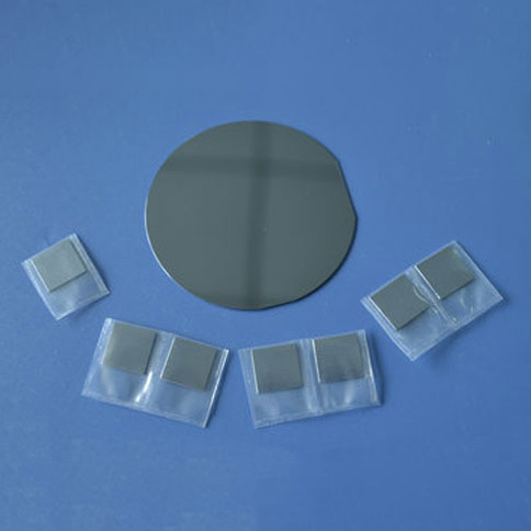
Gallium nitride, GaN substrate. GaN has a wide direct bandgap, strong atomic bonds and high thermal conductivity, etc., and it is a strong ability on anti-radiation, not only is the short-wavelength optoelectronic materials, also the replacement materials of high temperature semiconductor device. GaN can be used to make blue and green LED, or violet, ultraviolet light LD, ultraviolet detectors and high-frequency high-power electronic devices.
gallium nitride substrate is renowned for their exceptional properties, including a wide direct bandgap, strong atomic bonds, and high thermal conductivity. These characteristics make GaN an ideal material for a variety of advanced applications. It is particularly effective in resisting radiation, making it suitable for harsh environments. GaN substrates are widely used in the production of blue, green, and violet LEDs, as well as ultraviolet light-emitting diodes (LEDs), ultraviolet detectors, and high-frequency, high-power electronic devices. Additionally, GaN serves as an excellent replacement material for high-temperature semiconductor devices due to its superior thermal performance and robustness. As a leading China gallium nitride substrate supplier, we provide high-quality GaN substrates for a wide range of applications in the optoelectronics and semiconductor industries.

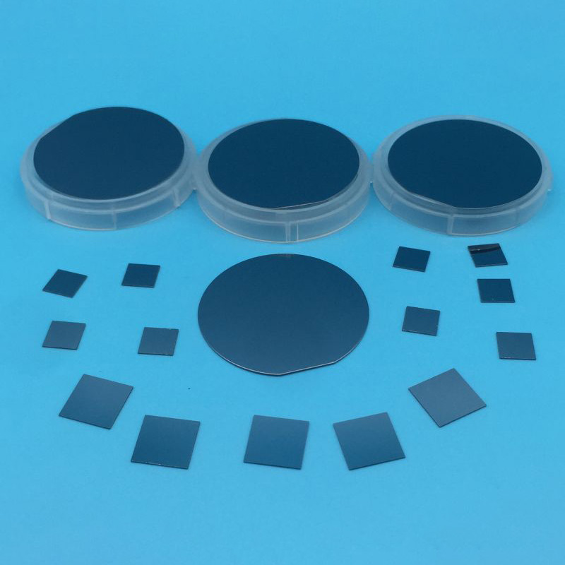
Gallium Nitride Substrate Specifications/cm
| Product Name | GaN single crystal substrate/wafer | |||
| Grade | S-level | A-level | B-level | C-level |
| Standard Size | 5X5.5mm, 10x10.5mm, 14x15mm, φ50.8mm, φ100mm | |||
| Standard Thickness | 350 ± 20 μm; 500 ± 20 μm | |||
| Marco Defect Density | < 0/cm² | < 0.3/cm² | < 1/cm² | < 4/cm² |
| Orientation | C-plane < 0001 >± 0.5° | |||
| Primary Orientation flat | < 1-100 >± 0.5°, 16mm(2-inch) / 30mm(4-inch) | |||
| Second Orientation flat | < 11-20 >± 3°, 8mm(2-inch) / 15mm(4-inch) | |||
| TTV | < = 15μm | |||
| BOW | < = 20μm | |||
| Dopant / Conductive | Undoped/N-type (Resistivity: < 0.5 Ω-cm) | |||
| Semi-insulating/Fe-doped (Resistivity: > 10E6 Ω-cm) | ||||
| Si-doped/N-type (Resistivity: < 0.05 Ω-cm ) | ||||
| Dislocation Density | < 3x106 cm-2 | < 3x106 cm-2 | < 3x106 cm-2 | |
| Useable surface area | > 90% | > 80% | > 70% | |
| Max size of macro defects | < 700 μm | < 2000 μm | < 4000 μm | |
| Polishing | Ga-face surface roughness: Ra < 0.3nm >(Epitaxy-ready) | |||
| N-face surface roughness: Ra 0.5 ~1.5 μm (optional: Ra < 0.3 nm(polished) | ||||
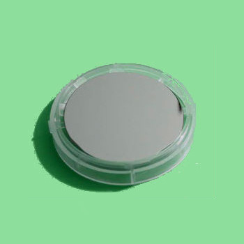
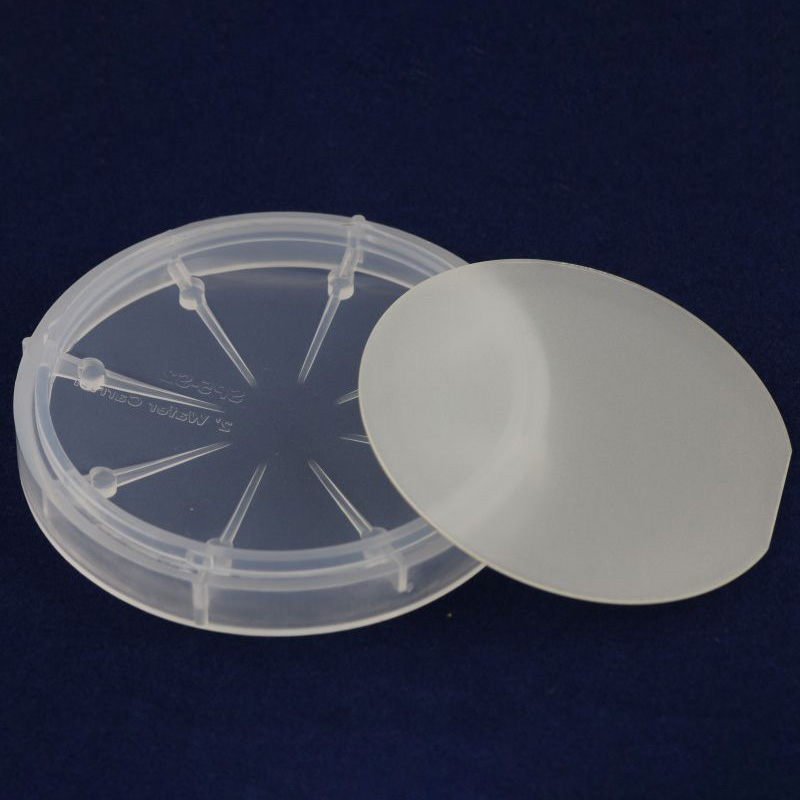
| Packing | Each piece individual packed in one bag, with class-100 clean bag | |||
Gallium Nitride Substrate Features
1. Wide Bandgap: GaN has a wide direct bandgap of approximately 3.4 eV, which allows it to operate efficiently at high voltages, temperatures, and frequencies, making it ideal for high-performance applications.
2. High Thermal Conductivity: GaN substrates offer superior heat dissipation, which is crucial for high-power devices. This property ensures better thermal management, reducing the risk of overheating in electronic components.
3. Radiation Resistance: GaN is highly resistant to radiation, which makes it suitable for use in space applications, high-energy physics experiments, and other environments exposed to radiation.
4. Mechanical Strength: GaN has strong atomic bonds, providing excellent mechanical strength and durability. This makes GaN substrates suitable for harsh operational conditions.
5. Optoelectronic Applications: GaN is widely used in the production of blue, green, and violet LEDs, as well as ultraviolet light-emitting diodes (LEDs), offering high luminous efficiency and long lifespan.
Gallium Nitride Substrate FAQ
What is Gallium Nitride (GaN) substrate?
GaN substrate is a semiconductor material known for its wide bandgap, high thermal conductivity, radiation resistance, and mechanical strength. It is used in optoelectronics, power electronics, and high-frequency applications.
What are the main applications of GaN substrates?
GaN substrates are primarily used in blue, green, and violet LEDs, ultraviolet light-emitting diodes (LEDs), power electronics, RF amplifiers, high-frequency devices, and radiation-resistant applications.
Why is GaN preferred for high-power electronics?
GaN has excellent thermal conductivity, high efficiency, and the ability to operate at high temperatures, which makes it ideal for high-power applications such as power converters and RF amplifiers.
How does GaN perform in high-temperature environments?
GaN can withstand higher temperatures compared to traditional semiconductor materials, making it ideal for high-temperature applications like automotive, aerospace, and energy systems.
Packaging and Transportation
The packaging should be able to withstand the impact, vibration, stacking and extrusion that may be encountered during transportation, while also it has to easy to load, unload and handle.
We use professional wafer box packaging. The wafer box is protected by a double layer bag, the inside is a PE bag that can be dust-proof, and the outside is a aluminum foil bag that can be isolated from the air. The two-layer bags are vacuum-packed.
We will choose carton models according to different sizes of products. And between the product and the carton filled with shock-proof EPE foam, play a comprehensive protection.
Finally choose air transport to reach the customer's hands. This allows customers in any country and region to receive the product in the fastest time.
We comply with the Material Safety Data Sheet (MSDS) rules to ensure that the products transported are free of harmful substances and will not cause environmental pollution and explosion and other possible hazards.

Enterprise Strength
Factory Area: 3000 sq
Process:
1. Shaping→2. Edge Profile→3. Lapping→4. Polishing→5. Cleaning→6. Packing→7. Transportation
Capacity:
Glass Wafer --- 30K pcs
Silicon Wafer --- 20K pcs
(Equal to 6in)

Quality Assurance
Quality inspection method: Product inspection in accordance with SEMI standard or according to customer's requirements, together with product COA.
Warranty period: In accordance with the contract requirements.
Quality system management:
●Organize production according to ISO9001 and other quality system standards.
Quality management system and measures:
●Establish a strict quality assurance system, the heads of all departments and quality engineers to ensure the coordinated operation of the quality system.
●Strengthen the quality inspection system, strengthen the process quality control
●Strict material quality control, ensure that the input materials meet the design requirements and technical specifications.
●Implement a timely filing system for technical data to ensure that all processing technical data is complete/accurate.
Quality control in the production stage:
●Production preparation stage: carefully organize relevant personnel to learn product drawings and technical rules, and improve the technical level of employees.
●Quality control of the production process: the implementation of a strict handover system, the previous step of the process to the next step of the transfer, should be detailed processing. At the same time, strengthen the quality inspection system to ensure the quality of each step of the process.
●Quality acceptance: All processes must be quality acceptance before proceeding to the next process.

Pre-sales and After-sales
Pre-sales Service
Professional technical support and commercial team to help you determine product specifications according to product use, and issue specifications.
On-purchase Service
Produce products according to the confirmed specifications and our process.
After Sale Service
We will respond to any product problems encountered by customers or process problems encountered by customers within 24 hours. We can choose from various forms of service, such as email, video conference and so on.
Plutosemi Co., Ltd. was established in 2019, headquartered in Nanhai, Foshan, focusing on the research and development, production, and sales of high-performance semiconductor materials.
Advanced production capacity: We have three major production bases in China, with a monthly production capacity of 100000 equivalent 6-inch silicon wafers and 30000 equivalent 8-inch glass wafers, ensuring stable and efficient product supply for our customers.
High quality products: We provide efficient and stable product supply innovative solutions in the fields of glass wafers, silicon polishing wafers, epitaxial wafers (EPI), silicon on insulator wafers (SOI), and more. Our silicon wafers have the characteristics of ultra-thin, ultraflat, and high-precision, which can meet the needs of various high-end applications. Our glass and quartz substrates are also renowned for their high smoothness and precise aperture design.