Indium Antimonide Substrate
Compound Semiconductor Wafers

-
+86-17701852595 WhatsApp
-
sales@plutosemitech.com Email
Indium antimonide (InSb) is a crystalline compound made from the elements indium (In) and antimony (Sb) with stable physicochemical properties and excellent process compatibility. It is a narrow-gap Group III-V semiconductor material used in infrared detectors, including thermal imaging cameras, FLIR systems, infrared guided missile systems and infrared astronomy. Indium antimonide detectors are sensitive between 1-5 μm wavelength. Indium antimonide is a very common detector in older single detector mechanically scanned thermal imaging systems. Another application is as a source of terahertz radiation, as it is an intense photo-dember emitter.
Physical Properties:
InSb has the appearance of dark grey silvery metallic particles or a powder with a glassy sheen. When heated above 500°C it melts and decomposes, releasing antimony and antimony oxide fumes. The crystal structure is sphalerite with a lattice constant of 0.648 nm.
Molecular weight: 236.58
Appearance: Dark grey metallic crystal
Melting point: 527°C
Density: 5.78g/cm3
Solubility in water: insoluble
Electronic Properties:
InSb is a narrow bandgap semiconductor with an energy bandgap of 0.17 eV at 300 K and 0.23 eV at 80 K. Except for carbon nanotubes, undoped InSb possesses a room temperature electron mobility (78,000 cm2/Vs), an electron drift velocity, and a trajectory length (up to 0.7 m at 300 K) higher than that of known semiconductor materials.
When exposed to infrared radiation, indium antimonide photodiode detectors generate a current.The internal quantum efficiency of InSb is practically 100%, but it varies with thickness, especially for near-band-edge photons. As with any narrow bandgap material, InSb detectors require periodic recalibration, which adds to the complexity of the imaging system. Where high sensitivity is required, such as in long-range military thermal imaging systems, the added complexity is worthwhile.InSb detectors must be operated at low temperatures and also need to be cooled (typically 80 K).
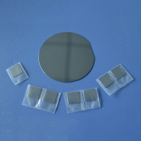
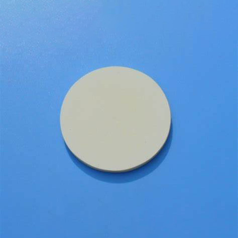
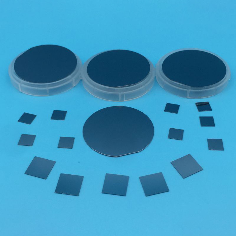
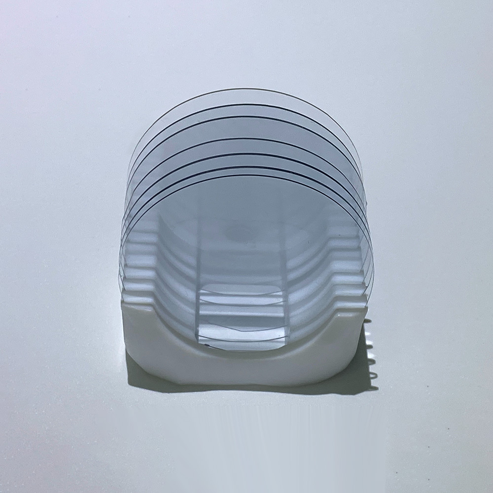
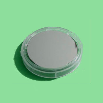
indium antimonide substrate is a high-performance material derived from the compound Indium Antimonide, known for its excellent crystalline structure and superior physical properties. It is commonly used as a base for the fabrication of infrared detectors and devices due to its narrow bandgap and optimal thermal conductivity. InSb substrates offer significant advantages in infrared sensor technology, especially in thermal imaging, FLIR systems, and infrared guidance systems. These substrates are also used in research for terahertz radiation applications, thanks to their intense photo-dember emission characteristics. PLOTOSEMI, as a China indium antimonide substrate supplier, offer high-quality InSb substrates with exceptional purity and surface quality, ideal for manufacturing advanced infrared sensors and detectors.

Indium Antimonide Substrate Specifications
| Monocrystalline | InSb | ||
| External Dimensions | 2”(50.8±0.3mm), 3”(76.2±0.3mm) | ||
| Thickness | 500/600±25um | ||
| Dopant | None | Te | Ge |
| Conductivity Type | N | N | P |
| Carrier Concentration(cm-3) | <3E15 | E17~E18 | 1~4×10 |
| Etch-Pit-Density(cm-2) | <2×10² | ||
Indium Antimonide Substrate Features
1. Narrow Bandgap: InSb has a small bandgap of approximately 0.17 eV at room temperature, making it highly suitable for infrared detection applications, particularly in the 1-5 μm wavelength range.
2. High Sensitivity: It is highly sensitive to infrared radiation, making it ideal for use in thermal imaging systems, infrared detectors, and FLIR (Forward Looking Infrared) systems.
3. Excellent Crystalline Structure: InSb substrates possess a high-quality crystalline structure that ensures efficient performance and minimal defects during the fabrication of infrared detectors.
4. Good Thermal Conductivity: InSb has excellent thermal conductivity, which aids in the efficient dissipation of heat, improving the performance and longevity of infrared sensor devices.
5. Photo-Dember Emission: InSb is a strong emitter of terahertz radiation due to its intense photo-dember effect, which makes it useful in applications requiring terahertz generation.
Indium Antimonide Substrate FAQ
What is Indium Antimonide (InSb) substrate used for?
InSb substrates are primarily used in the fabrication of infrared detectors, thermal imaging systems, FLIR cameras, and infrared-guided missile systems. They are also used in terahertz radiation applications.
How sensitive is InSb to infrared radiation?
InSb is highly sensitive to infrared radiation, especially in the 1-5 μm range, making it ideal for thermal imaging and other infrared detection applications.
What industries use InSb substrates?
InSb substrates are used across various industries, including defense, aerospace, medical imaging, scientific research, and infrared technology, such as FLIR systems and infrared astronomy.
Can InSb substrates be customized?
Yes, InSb substrates are available in various sizes, thicknesses, and surface finishes, allowing for customization to meet specific application requirements.
Plutosemi Co., Ltd. was established in 2019, headquartered in Nanhai, Foshan, focusing on the research and development, production, and sales of high-performance semiconductor materials.
Advanced production capacity: We have three major production bases in China, with a monthly production capacity of 100000 equivalent 6-inch silicon wafers and 30000 equivalent 8-inch glass wafers, ensuring stable and efficient product supply for our customers.
High quality products: We provide efficient and stable product supply innovative solutions in the fields of glass wafers, silicon polishing wafers, epitaxial wafers (EPI), silicon on insulator wafers (SOI), and more. Our silicon wafers have the characteristics of ultra-thin, ultraflat, and high-precision, which can meet the needs of various high-end applications. Our glass and quartz substrates are also renowned for their high smoothness and precise aperture design.