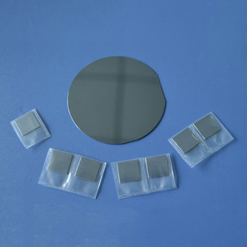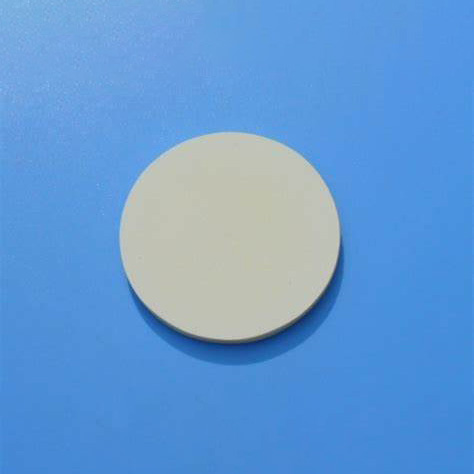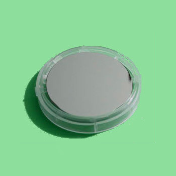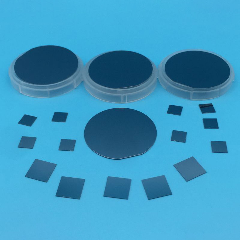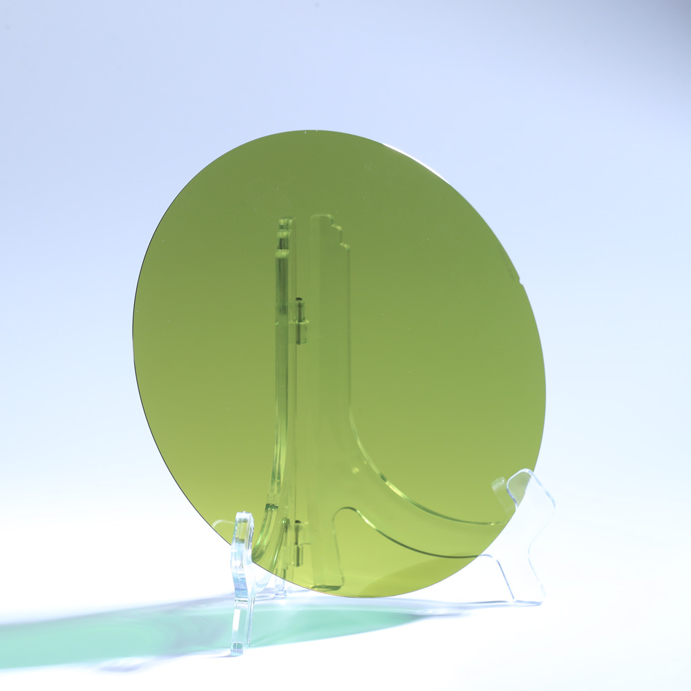
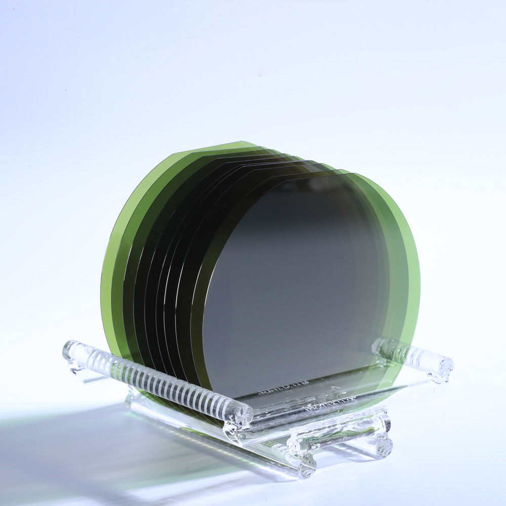
SiC Silicon Carbide Wafer
Compound Semiconductor Wafers

-
+86-17701852595 WhatsApp
-
sales@plutosemitech.com Email
Silicon Carbide Wafer is a compound semiconductor material composed of silicon and carbon elements, with the chemical formula SiC. As a high-performance wide-bandgap semiconductor material, SiC Wafer exhibits excellent performance in high-temperature, high-voltage and high-power applications, and is an ideal choice for next-generation power electronics and radio frequency devices. With the growing global demand for high-efficiency, low-energy devices, SiC Wafer has a very broad market prospect and has become one of the key materials to promote the advancement of semiconductor technology.

SiC Silicon Carbide Wafer Specifications
| Diameter | 150±0.5mm, 200±0.25 mm | ||
| Thickness 4H | 350 μm±25μm | ||
| 500 μm±25μm | |||
| Wafer Orientation | Off axis : 4.0° toward 1120 ±0.5° | ||
| Micropipe Density | ≤ 0.2 cm-2 | ≤ 5 cm-2 | ≤ 10 cm-2 |
| BPD | ≤ 1500ea/cm2 | ≤ 2000ea/cm2 | NA |
| TSD | ≤ 300ea/cm2 | ≤ 1000ea/cm2 | NA |
| Resistivity | 0.015~0.025 Ω·cm | ||
| Edge exclusion | 3 mm | ||
| TTV/Bow /Warp | ≤ 3μm / ≤ 5μm / ≤ 10μm | ||
| Roughness | Polish Ra ≤ 0.2 nm | ||
| Cracks by high intensity light | None | None | 1 allowed, ≤ 1 mm |
| Hex Plates by high intensity light | Cumulative area≤ 1 % | Cumulative area≤ 1 % | Cumulative area≤ 3 % |
| Polytype Areas by high intensity light | None | Cumulative area≤ 2 % | Cumulative area≤ 5% |
| Scratches by | 3 scratches to 1× | 5 scratches to 1× | 8 scratches to 1× |
| high intensity light | wafer diameter | wafer diameter | wafer diameter |
| cumulative length | cumulative length | cumulative length | |
| Edge chip | None | 3 allowed, ≤ 0.5 mm each | 5 allowed, ≤ 1 mm each |
| Contamination by | None | ||
| high intensity light | |||
| OEM/ODM | Accept | ||
| Compay Nature | China Manufacturers Suppliers Factory | ||
SiC Silicon Carbide Wafer Features
1. Wide bandgap characteristics:
The core feature of Silicon Carbide Wafer is its wide bandgap characteristics, with a bandgap width of about 3.26 eV, which is much higher than that of traditional silicon materials (about 1.12 eV). This feature gives SiC Wafer extremely high breakdown electric field strength and thermal conductivity, enabling it to work stably in high temperature and high pressure environments. Under the same conditions, the power density of SiC devices can be more than an order of magnitude higher than that of silicon devices, thereby significantly improving the efficiency and reliability of the equipment.
2. High thermal conductivity:
The thermal conductivity of Silicon Carbide Wafer is as high as 490 W/m·K, which is more than three times that of silicon materials (about 150 W/m·K). This excellent heat dissipation performance enables SiC devices to operate for a long time in high temperature environments without the need for additional cooling devices. This is particularly important for application scenarios that require high power density, such as electric vehicles, industrial power supplies, and renewable energy systems.
3. High breakdown voltage:
Silicon Carbide Wafer has a much higher breakdown voltage than silicon, which means that SiC-based power devices can operate at higher voltages while maintaining low leakage current. This feature makes SiC devices perform well in areas such as power conversion, motor drives, and solar inverters, significantly reducing energy losses and improving system efficiency.
4. Low on-resistance:
Silicon Carbide Wafer has a much lower on-resistance than silicon, which makes SiC-based power devices generate less heat in the on state, further improving the overall efficiency of the system. This low on-resistance feature is particularly suitable for high-frequency switching applications, which can significantly reduce switching losses.
5. High mechanical strength:
Silicon Carbide Wafer has extremely high mechanical strength, and its hardness is second only to diamond and more than twice that of silicon. This feature makes SiC Wafer exhibit excellent wear and scratch resistance during processing, while also maintaining structural integrity in extreme environments (such as high temperature, high pressure or strong vibration).
6. Chemical stability:
SiC Wafer shows extremely high stability to most chemicals and can maintain good performance even in strong acid, strong alkali or high temperature oxidizing environments. This chemical stability not only extends the service life of the device, but also reduces maintenance costs.
7. Low dielectric constant:
SiC Wafer has a low dielectric constant of only 9.7, which is much lower than silicon materials (about 11.7). This feature allows SiC devices to show lower parasitic capacitance in high-frequency applications, thereby significantly improving signal transmission speed and circuit response time.
8. High radiation tolerance:
SiC Wafer has extremely high tolerance to radiation and can maintain stable electrical performance in high radiation environments. This feature makes it have a wide range of application potential in aerospace, nuclear energy and military fields.
9. Precise crystal quality control:
Plutosemi's SiC Silicon Carbide Wafer uses advanced crystal growth technology and precision processing technology to ensure that each wafer has extremely high crystal quality and surface flatness. For example, the micropipe density is controlled at an extremely low level (≤0.2 cm⁻²), and there are no cracks or impurities inside the crystal, ensuring the reliability and consistency of the device.
10. Customized specifications:
Plutosemi provides SiC Wafers of various specifications, including products with diameters of 150 mm and 200 mm, with thicknesses ranging from 350 μm to 500 μm, to meet the needs of different customers. In addition, the orientation angle (Off-axis) and edge exclusion area (Edge exclusion) of the Wafer are also strictly controlled to ensure compliance with industry standards.
SiC Silicon Carbide Wafer Process Flow
1. Raw material preparation:
The production of SiC Silicon Carbide Wafer begins with the selection of high-purity silicon powder and carbon source (such as graphite). These raw materials need to undergo rigorous purification to remove any impurities that may affect the quality of the crystal. Only raw materials with a purity of 99.999% can enter the subsequent production process.
2. Crystal growth:
The crystal growth of SiC Wafer usually adopts physical vapor transport (PVT), which is a mature crystal growth technology. During the PVT process, silicon powder and carbon source are heated to high temperatures (about 2000°C to 2500°C) to form a gas phase reaction, and finally deposited on the seed crystal to form a SiC single crystal. The entire growth process needs to be carried out in a vacuum or inert gas environment to avoid external contamination.
3. Temperature and pressure control:
During the crystal growth process, precise control of temperature and pressure is crucial. Plutosemi uses advanced temperature control systems and pressure regulators to ensure that the temperature and pressure in the reactor are always kept at the optimal state, thereby generating high-quality SiC crystals.
4. Crystal cutting and grinding:
After the crystal growth is completed, the original SiC ingot will be cut into thin wafers. Plutosemi uses high-precision cutting equipment to ensure that the thickness of the wafer is uniform (the error is controlled within ±25 μm). The cut wafer also needs to go through multiple grinding processes to achieve the surface flatness and roughness requirements.
5. Polishing and cleaning:
Polishing is a key step in SiC wafer production, aiming to further improve the surface quality of the wafer. Plutosemi uses chemical mechanical polishing (CMP) technology to control the surface roughness of the wafer to Ra ≤ 0.2 nm. After polishing, the wafer also needs to go through a rigorous cleaning process to remove residual particles and contaminants.
6. Quality inspection:
Each SiC wafer needs to undergo multiple quality inspections before leaving the factory, including micropipe density detection, surface defect analysis, resistivity measurement, and optical performance evaluation. Plutosemi uses advanced testing equipment such as scanning electron microscopes (SEM) and atomic force microscopes (AFM) to ensure that wafers meet strict industry standards.
7. Packaging and transportation:
In order to prevent wafers from being damaged during transportation, Plutosemi uses professional anti-static and shockproof packaging solutions. Wafers are placed in a dedicated protective box and fixed with cushioning materials to ensure that they remain intact during transportation.
SiC Silicon Carbide Wafer Application
1. Power Electronic Devices:
SiC Silicon Carbide Wafer is the core material for manufacturing high-performance power electronic devices, which are widely used in power conversion, motor drive and power management. SiC-based MOSFET and IGBT devices can operate at higher voltages and frequencies, significantly reducing energy losses and improving system efficiency. This feature makes it an ideal choice for electric vehicles, industrial power supplies and renewable energy systems such as wind power generation and solar inverters.
2. RF Devices:
Silicon Carbide Wafer's high thermal conductivity and wide bandgap characteristics make it an ideal material for RF devices. SiC-based RF power amplifiers and mixers can maintain stable performance under high frequency and high power conditions and are widely used in communication base stations, radar systems and satellite communications.
3. Aerospace and Defense:
SiC Wafer's high radiation tolerance and excellent mechanical strength make it an important application in the aerospace and defense fields. For example, SiC-based sensors and actuators can work stably in extreme environments and are used in attitude control, navigation and communication systems of spacecraft.
4. New energy and energy storage:
In the field of new energy, SiC Wafer is widely used in equipment such as photovoltaic inverters, energy storage systems and charging piles. Its high efficiency and high reliability can significantly improve energy conversion efficiency and reduce system costs.
5. Automotive electronics:
SiC Wafer is one of the core materials for electric vehicles and hybrid vehicles, and is used in components such as on-board chargers, DC/DC converters and traction inverters. SiC-based devices can significantly reduce energy loss, extend battery life, and improve the overall performance of the vehicle.
6. Industrial automation:
In the field of industrial automation, SiC Wafer is used in high-voltage DC transmission, industrial motor drives and smart grid systems. Its high power density and high efficiency characteristics can significantly improve the performance and reliability of industrial equipment.
7. Scientific research and development:
SiC Silicon Carbide Wafer is also an important material for scientific research and development. It is widely used in the research and development of new semiconductor devices, performance testing of wide bandgap materials and exploration of future technologies.
Packaging and Transportation
The packaging should be able to withstand the impact, vibration, stacking and extrusion that may be encountered during transportation, while also it has to easy to load, unload and handle.
We use professional wafer box packaging. The wafer box is protected by a double layer bag, the inside is a PE bag that can be dust-proof, and the outside is a aluminum foil bag that can be isolated from the air. The two-layer bags are vacuum-packed.
We will choose carton models according to different sizes of products. And between the product and the carton filled with shock-proof EPE foam, play a comprehensive protection.
Finally choose air transport to reach the customer's hands. This allows customers in any country and region to receive the product in the fastest time.
We comply with the Material Safety Data Sheet (MSDS) rules to ensure that the products transported are free of harmful substances and will not cause environmental pollution and explosion and other possible hazards.

Enterprise Strength
Factory Area: 3000 sq
Process:
1. Shaping→2. Edge Profile→3. Lapping→4. Polishing→5. Cleaning→6. Packing→7. Transportation
Capacity:
Glass Wafer --- 30K pcs
Silicon Wafer --- 20K pcs
(Equal to 6in)

Quality Assurance
Quality inspection method: Product inspection in accordance with SEMI standard or according to customer's requirements, together with product COA.
Warranty period: In accordance with the contract requirements.
Quality system management:
●Organize production according to ISO9001 and other quality system standards.
Quality management system and measures:
●Establish a strict quality assurance system, the heads of all departments and quality engineers to ensure the coordinated operation of the quality system.
●Strengthen the quality inspection system, strengthen the process quality control
●Strict material quality control, ensure that the input materials meet the design requirements and technical specifications.
●Implement a timely filing system for technical data to ensure that all processing technical data is complete/accurate.
Quality control in the production stage:
●Production preparation stage: carefully organize relevant personnel to learn product drawings and technical rules, and improve the technical level of employees.
●Quality control of the production process: the implementation of a strict handover system, the previous step of the process to the next step of the transfer, should be detailed processing. At the same time, strengthen the quality inspection system to ensure the quality of each step of the process.
●Quality acceptance: All processes must be quality acceptance before proceeding to the next process.

Pre-sales and After-sales
Pre-sales Service
Professional technical support and commercial team to help you determine product specifications according to product use, and issue specifications.
On-purchase Service
Produce products according to the confirmed specifications and our process.
After Sale Service
We will respond to any product problems encountered by customers or process problems encountered by customers within 24 hours. We can choose from various forms of service, such as email, video conference and so on.
Plutosemi Co., Ltd. was established in 2019, headquartered in Nanhai, Foshan, focusing on the research and development, production, and sales of high-performance semiconductor materials.
Advanced production capacity: We have three major production bases in China, with a monthly production capacity of 100000 equivalent 6-inch silicon wafers and 30000 equivalent 8-inch glass wafers, ensuring stable and efficient product supply for our customers.
High quality products: We provide efficient and stable product supply innovative solutions in the fields of glass wafers, silicon polishing wafers, epitaxial wafers (EPI), silicon on insulator wafers (SOI), and more. Our silicon wafers have the characteristics of ultra-thin, ultraflat, and high-precision, which can meet the needs of various high-end applications. Our glass and quartz substrates are also renowned for their high smoothness and precise aperture design.