Single Crystal Strontium Titanate Substrate
Compound Semiconductor Wafers

-
+86-17701852595 WhatsApp
-
sales@plutosemitech.com Email
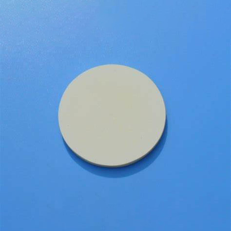
The Single Crystal Strontium Titanate Substrate (SrTiO3) is the preferred material for high-temperature superconducting thin films due to its exceptional lattice matching with materials like YBaCuO. With no twin structure and excellent physical, mechanical, and thermal properties, SrTiO3 substrates ensure superior performance in demanding applications. They support various thin-film production techniques, including magnetron sputtering, pulsed laser deposition, and laser molecular beam epitaxy, enabling the creation of high-temperature superconducting films with TCO ≥ 90 °K and JCO ≥ 10⁶ A/cm². Surface finish options include fine ground, single-side polished, or double-side polished, with roughness as low as Ra<5å>China strontium titanate substrate manufacturer, we are committed to providing high-quality SrTiO3 substrates tailored to meet the needs of advanced research and industrial applications.

Product Standard:
| Product Name | Orientation | Standard Size | Thickness | Polishing |
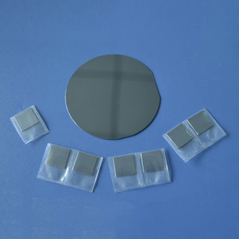
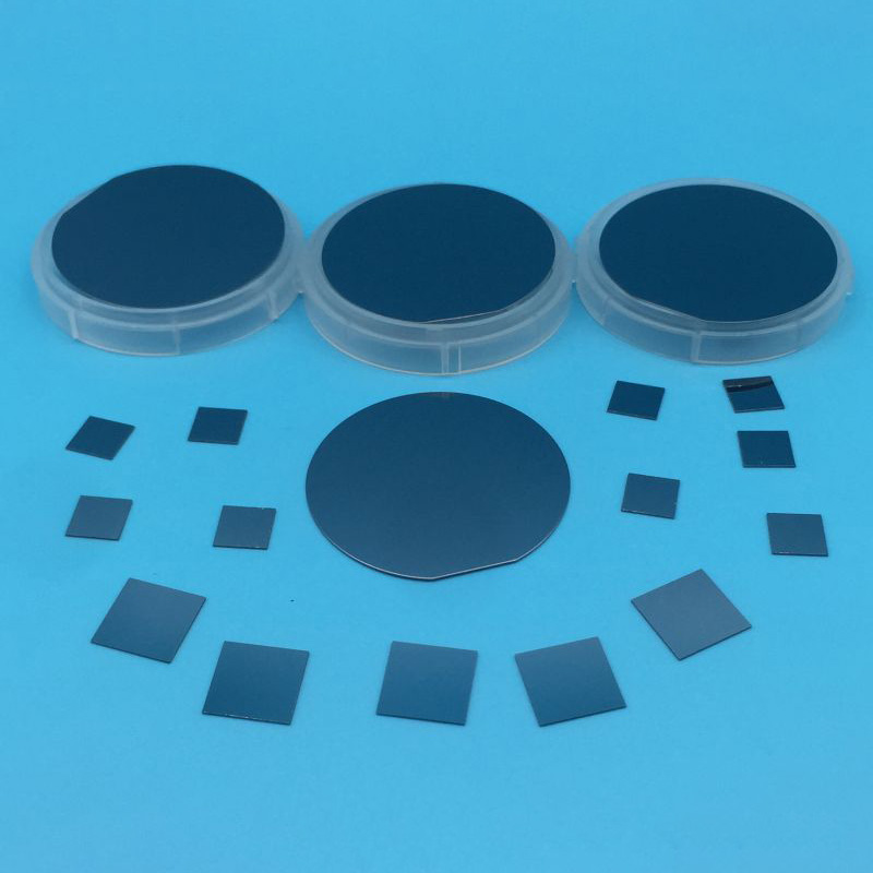
| SrTiO3 substrate | <100>±0.5° <110>±0.5° <111>±0.5° Or other off-angle | 10x10mm 10x5mm 5x5mm 3x3mm 20x20mm φ1"x0.5mm Or others | 0.1mm 0.2mm 0.5mm 1.0mm 2.0mm Or others | Fine ground Single side polished Double side polished Roughness: Ra<5a(0.5n)<> |
Single Crystal Strontium Titanate Substrate Specifications
| Product Name | Strontium titanate(SrTiO3) single crystal substrate/wafer |
| Crystal structure | Cubic |
| Growth method | Vernuil |
| Lattice constant | a = 3.905Å |
| Melting point | 2080℃ |
| Density | 5.175 (g/cm³) |
| Mohs Hardness | 6 |
| Coefficient of thermal expansion (/ ℃) | 10.4 × 10⁻⁶ |
| Dielectric constant | ~300 |
| Chemical stability | Insoluble in water |
| Loss tangent | ~ 5 x 10⁻⁴(300k) ~ 3 x 10⁻⁴(77k) |
| Appearance | Translucent |
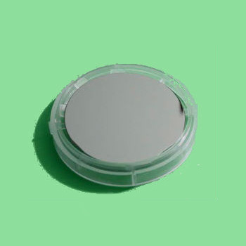
| Package | Each pieces packed in 100 clean bag with 1000 clean room |
Single Crystal Strontium Titanate Substrate Features
1. Exceptional Lattice Matching
Perfect compatibility with high-temperature superconducting materials like YBaCuO. Enables the formation of high-quality thin films with superior performance.
2. High-Temperature Superconductivity
Supports films with critical temperature (TCO) ≥ 90 °K. Achieves critical current density (JCO) ≥ 10A/cm2.
3. High Purity and Structural Integrity
Single crystal structure with no twin boundaries. Provides excellent physical, mechanical, and thermal properties.
4. Versatile Film Formation Techniques
Suitable for magnetron sputtering, pulsed laser deposition, and laser molecular beam epitaxy. Ensures uniform and defect-free thin film production.
5. Customizable Specifications
Multiple orientations:<100>,<110>,<111>, and other off-angles. Available in various standard sizes (e.g., 10x10mm, 5x5mm, 3x3mm) and thicknesses (0.1mm to 2.0mm). Options for fine ground, single-side polished, or double-side polished surfaces.
Single Crystal Strontium Titanate Substrate FAQ
What is a Strontium Titanate (SrTiO3) substrate used for?
SrTiO3 substrates are widely used in high-temperature superconducting thin films, oxide electronics, and junction technology due to their exceptional lattice matching and structural properties.
What are the typical thickness options for SrTiO3 substrates?
Standard thicknesses range from 0.1mm to 2.0mm, with the option for custom thicknesses based on specific requirements.
What surface polishing options are available?
SrTiO3 substrates can be fine ground, single-side polished, or double-side polished, with surface roughness as low as Ra<5?>
Which deposition techniques are compatible with SrTiO3 substrates?
SrTiO3 supports various techniques, including magnetron sputtering, pulsed laser deposition (PLD), and laser molecular beam epitaxy.
Packaging and Transportation
The packaging should be able to withstand the impact, vibration, stacking and extrusion that may be encountered during transportation, while also it has to easy to load, unload and handle.
We use professional wafer box packaging. The wafer box is protected by a double layer bag, the inside is a PE bag that can be dust-proof, and the outside is a aluminum foil bag that can be isolated from the air. The two-layer bags are vacuum-packed.
We will choose carton models according to different sizes of products. And between the product and the carton filled with shock-proof EPE foam, play a comprehensive protection.
Finally choose air transport to reach the customer's hands. This allows customers in any country and region to receive the product in the fastest time.
We comply with the Material Safety Data Sheet (MSDS) rules to ensure that the products transported are free of harmful substances and will not cause environmental pollution and explosion and other possible hazards.

Enterprise Strength
Factory Area: 3000 sq
Process:
1. Shaping→2. Edge Profile→3. Lapping→4. Polishing→5. Cleaning→6. Packing→7. Transportation
Capacity:
Glass Wafer --- 30K pcs
Silicon Wafer --- 20K pcs
(Equal to 6in)

Quality Assurance
Quality inspection method: Product inspection in accordance with SEMI standard or according to customer's requirements, together with product COA.
Warranty period: In accordance with the contract requirements.
Quality system management:
●Organize production according to ISO9001 and other quality system standards.
Quality management system and measures:
●Establish a strict quality assurance system, the heads of all departments and quality engineers to ensure the coordinated operation of the quality system.
●Strengthen the quality inspection system, strengthen the process quality control
●Strict material quality control, ensure that the input materials meet the design requirements and technical specifications.
●Implement a timely filing system for technical data to ensure that all processing technical data is complete/accurate.
Quality control in the production stage:
●Production preparation stage: carefully organize relevant personnel to learn product drawings and technical rules, and improve the technical level of employees.
●Quality control of the production process: the implementation of a strict handover system, the previous step of the process to the next step of the transfer, should be detailed processing. At the same time, strengthen the quality inspection system to ensure the quality of each step of the process.
●Quality acceptance: All processes must be quality acceptance before proceeding to the next process.

Pre-sales and After-sales
Pre-sales Service
Professional technical support and commercial team to help you determine product specifications according to product use, and issue specifications.
On-purchase Service
Produce products according to the confirmed specifications and our process.
After Sale Service
We will respond to any product problems encountered by customers or process problems encountered by customers within 24 hours. We can choose from various forms of service, such as email, video conference and so on.
Plutosemi Co., Ltd. was established in 2019, headquartered in Nanhai, Foshan, focusing on the research and development, production, and sales of high-performance semiconductor materials.
Advanced production capacity: We have three major production bases in China, with a monthly production capacity of 100000 equivalent 6-inch silicon wafers and 30000 equivalent 8-inch glass wafers, ensuring stable and efficient product supply for our customers.
High quality products: We provide efficient and stable product supply innovative solutions in the fields of glass wafers, silicon polishing wafers, epitaxial wafers (EPI), silicon on insulator wafers (SOI), and more. Our silicon wafers have the characteristics of ultra-thin, ultraflat, and high-precision, which can meet the needs of various high-end applications. Our glass and quartz substrates are also renowned for their high smoothness and precise aperture design.