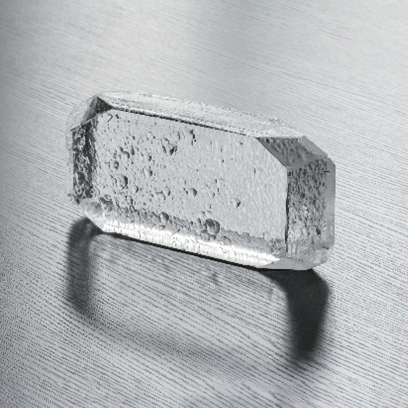

AF32 eco and AF35G Glass Wafer
Glass Wafer

-
+86-17701852595 WhatsApp
-
sales@plutosemitech.com Email
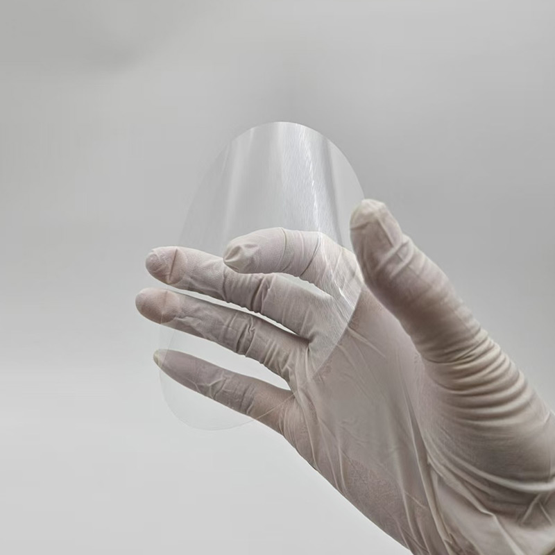
The AF32 eco Glass Wafer is a high-performance substrate designed for precision applications in the semiconductor and electronics industries. Available in sizes ranging from 2 to 12 inches, or customized to specific requirements, the wafer features a base material of SiO2 and is manufactured using the advanced Down-Draw growth method. The wafer is processed in a hundred-class clean room environment to ensure minimal contamination. It is RoHS-compliant, guaranteeing its suitability for eco-friendly and regulatory-compliant applications. The surface finishes are available in DSP (Double Side Polished), SSP (Single Side Polished), and DSL (Double Side Lapped), ensuring optimal surface quality for various device fabrication processes. Whether for research, development, or large-scale production, the AF32 eco Glass Wafer provides reliable performance and precision. As a trusted China AF32 eco glass wafer manufacturer, we offer high-quality wafers suitable for a wide range of semiconductor applications.

AF32 eco and AF35G Glass Wafer Specifications
| Optical Property | |||
Refractiive Index (nd (λ587.6 nm)) | Abbe Numbe r(ve = (ne– 1) / (nF‘ – nC‘)) | Dispersion | Stress Photoelastic Coefficien (in (nm/cm)/MPa) |
| 1.52 | 62.4 | 1.5156 | 31.6 |
| Thermal Property | |
| Item | Value |
| Coefficient of Linear Thermal Expansion α(20 - 300 °C) | 3.2x10⁻⁶ K-1 * |
| Specific Heat Capacity Cp(20 - 100 °C) | 0.8 kJ/(kg·K) |
| Transformation temperature in ℃ | 717 |
| Mechanical Property | |
| Item | Value |
| Density ρ (25 °C) | 2.43 g/cm3 |
| Torsion Modulus G | 30 kN/mm2 |
| Poisson's ratio | 0.24 |
| Knoop Hardness HK0.1/2 | 490 |
| Vickers hardness HK0.2/25 | 540 |
| Electrical Property | ||
| Item | Value | |
| Dielectric Constant(εr) (25℃,1 MHz) | 5.1 | |
| Leakage Constant(tanδ) (25℃,1 MHz) | 28×10-4 | |
| Electric Volume Resistivity (Ω·cm alternate current 50 Hz) | 250℃ | 7.9*1011 |
| 350℃ | 1.1*1010 | |
| Thermal Property | |
| Item | Value |
| Coefficient of Linear Thermal Expansion α(20 - 300 °C) | 3.25 x 10⁻⁶ K-1 * |
| Specific Heat Capacity Cp(20 - 100 °C) | 0.83 kJ/(kg·K) |
| Thermal Conductivity λ (90 °C) | 1.2 W/(m·K) |
| Technical Specifications | |||||||
| Diameter | 2inch | 3inch | 4inch | 5inch | 6inch | 8inch | 12inch |
| Thickness (um) | Depends on Request | ||||||
| Material | AF32eco & AF35G | ||||||
| Grade/Brand | SCHOTT | ||||||
| Surface Finished | DSP、SSP、DSL | ||||||
| TTV (um) | <5 | <5 | <5 | <5 | <5 | <10 | <15 |
| Bow/Warp (um) | <20 | <20 | <30 | <30 | <30 | <40 | <60 |
| Ra (nm) | <1 | ||||||
| S/D (um) | 40/20 | ||||||
AF32 eco and AF35G Glass Wafer Features
1. High-Quality Material (SiO2 Base): Both the AF32eco and AF35G Glass Wafers are made from premium SiO2 (silicon dioxide), ensuring excellent optical clarity, thermal stability, and electrical insulation properties.
2. Advanced Growth Method (Down-Draw): These wafers are manufactured using the advanced Down-Draw growth method, which ensures uniformity and consistency in size and quality.
3. Customizable Sizes: Available in a wide range of sizes, including 2-inch, 3-inch, 4-inch, 6-inch, 8-inch, and 12-inch diameters. Custom sizes can also be produced to meet specific client requirements.
4. Precision Surface Finishing: The wafers feature a variety of surface finishes, including DSP (Double Side Polished), SSP (Single Side Polished), and DSL (Double Side Lapped), ensuring the highest levels of surface quality for precision applications.
5. Clean Room Processing: Manufactured in a hundred-class clean room to minimize contamination, ensuring the wafers meet the strictest standards for purity and quality.
AF32 eco and AF35G Glass Wafer FAQ
What is the material used for AF32eco and AF35G Glass Wafers?
Both wafers are made from high-quality SiO2 (silicon dioxide), offering excellent optical clarity, thermal stability, and electrical insulation.
What sizes are available for AF32eco and AF35G Glass Wafers?
These wafers are available in sizes ranging from 2-inch to 12-inch in diameter, with custom sizes available upon request.
What surface finishes are available for these wafers?
The wafers are available with three surface finishes: DSP (Double Side Polished), SSP (Single Side Polished), and DSL (Double Side Lapped), allowing for various application needs.
Are the AF32eco and AF35G Glass Wafers suitable for semiconductor applications?
Yes, both wafers are ideal for semiconductor, MEMS, and optical device applications, offering excellent reliability and performance in these industries.
Packaging and Transportation
The packaging should be able to withstand the impact, vibration, stacking and extrusion that may be encountered during transportation, while also it has to easy to load, unload and handle.
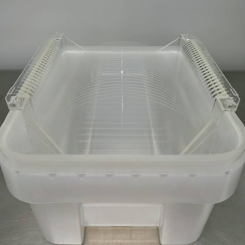
We use professional wafer box packaging. The wafer box is protected by a double layer bag, the inside is a PE bag that can be dust-proof, and the outside is a aluminum foil bag that can be isolated from the air. The two-layer bags are vacuum-packed.
We will choose carton models according to different sizes of products. And between the product and the carton filled with shock-proof EPE foam, play a comprehensive protection.
Finally choose air transport to reach the customer's hands. This allows customers in any country and region to receive the product in the fastest time.
We comply with the Material Safety Data Sheet (MSDS) rules to ensure that the products transported are free of harmful substances and will not cause environmental pollution and explosion and other possible hazards.

Enterprise Strength
Factory Area: 3000 sq
Process:
1. Shaping→2. Edge Profile→3. Lapping→4. Polishing→5. Cleaning→6. Packing→7. Transportation
Capacity:
Glass Wafer --- 30K pcs
Silicon Wafer --- 20K pcs
(Equal to 6in)

Quality Assurance
Quality inspection method: Product inspection in accordance with SEMI standard or according to customer's requirements, together with product COA.
Warranty period: In accordance with the contract requirements.
Quality system management:
●Organize production according to ISO9001 and other quality system standards.
Quality management system and measures:
●Establish a strict quality assurance system, the heads of all departments and quality engineers to ensure the coordinated operation of the quality system.
●Strengthen the quality inspection system, strengthen the process quality control
●Strict material quality control, ensure that the input materials meet the design requirements and technical specifications.
●Implement a timely filing system for technical data to ensure that all processing technical data is complete/accurate.
Quality control in the production stage:
●Production preparation stage: carefully organize relevant personnel to learn product drawings and technical rules, and improve the technical level of employees.
●Quality control of the production process: the implementation of a strict handover system, the previous step of the process to the next step of the transfer, should be detailed processing. At the same time, strengthen the quality inspection system to ensure the quality of each step of the process.
●Quality acceptance: All processes must be quality acceptance before proceeding to the next process.

Pre-sales and After-sales
Pre-sales Service
Professional technical support and commercial team to help you determine product specifications according to product use, and issue specifications.
On-purchase Service
Produce products according to the confirmed specifications and our process.
After Sale Service
We will respond to any product problems encountered by customers or process problems encountered by customers within 24 hours. We can choose from various forms of service, such as email, video conference and so on.
Plutosemi Co., Ltd. was established in 2019, headquartered in Nanhai, Foshan, focusing on the research and development, production, and sales of high-performance semiconductor materials.
Advanced production capacity: We have three major production bases in China, with a monthly production capacity of 100000 equivalent 6-inch silicon wafers and 30000 equivalent 8-inch glass wafers, ensuring stable and efficient product supply for our customers.
High quality products: We provide efficient and stable product supply innovative solutions in the fields of glass wafers, silicon polishing wafers, epitaxial wafers (EPI), silicon on insulator wafers (SOI), and more. Our silicon wafers have the characteristics of ultra-thin, ultraflat, and high-precision, which can meet the needs of various high-end applications. Our glass and quartz substrates are also renowned for their high smoothness and precise aperture design.