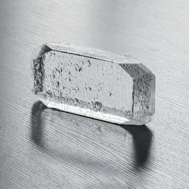

Fused Silica JGS1 Glass Wafer
Glass Wafer

-
+86-17701852595 WhatsApp
-
sales@plutosemitech.com Email
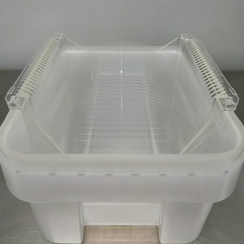
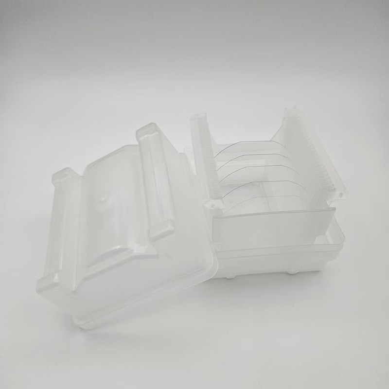
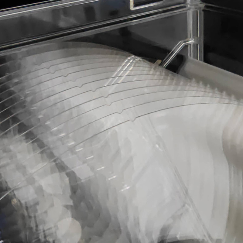
The Fused Silica JGS1 Glass Wafer is a high-performance material widely used in precision applications. Available in sizes ranging from 2 to 12 inches (custom sizes also available), it offers exceptional optical clarity and thermal stability. Made from high-purity SiO2, this wafer exhibits a low density of 2.2g/cm3 and a high melting point of 1730°C. It can safely withstand continuous operating temperatures of 1000-1100°C and short-term exposure to temperatures up to 1400°C. Its Moh's hardness rating of 7 ensures durability, while its resistance to rapid temperature changes (800-1100°C) makes it suitable for a variety of industrial applications. The wafer also boasts a thermal expansion coefficient of 5.4×10^-7 and a dielectric constant of 3.7 at normal temperatures, making it an ideal choice for electronics, semiconductor, and photonics industries. As a leading China JGS1 Glass Wafer supplier, we specialize in providing high-quality fused silica wafers with superior optical and thermal properties.

Product Name: Fused Silica JGS1 Glass Wafer
Size: 2/4/6/8/12inch or customized
Package: Hundred-class clean room
Customized Support: YES
RoHS: YES
Delivery Methods: Logistics Express
Marketable Area: oversea
Growth Method: Gas refining method/Synthesis
Base: SiO2
Density: 2.2g/cm3
Melting Point: 1730℃
Moh's Hardness: 7
Maximum safe operating temperature (continuous): 1000-1100℃
Maximum safe operating temperature (short time): 1300-1400℃
Resistance to rapid change in temperature: 800-1100℃
Thermal Expansion Coefficient: 5.4×10⁻⁷
Dislectric Constant(0~106 Hz): 3.7(Normal Temperatures)
Conductivity(S/m): 10-17~10-16(20℃)
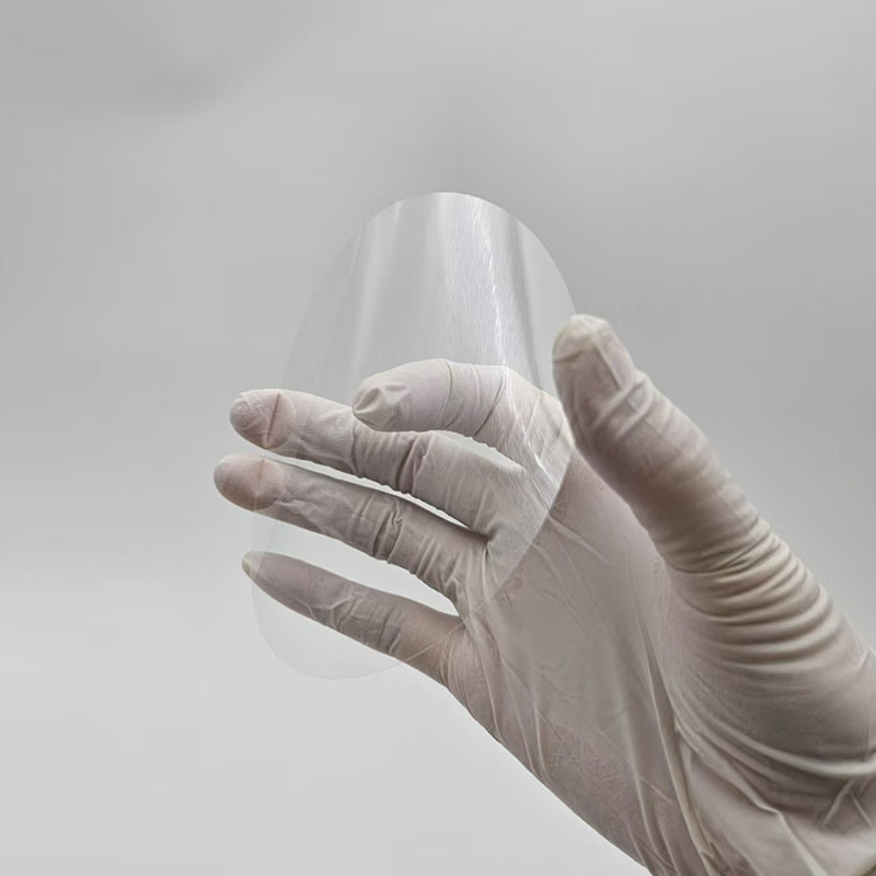
Color: Transparent
Fused Silica JGS1 Glass Wafer Specifications
| Grade | Product Name | Applied spectral band range(um) |
| JGS1 | Fused Silica Glass Wafer | 0.185-2.5 |
Fused Silica JGS1 Glass Wafer Transmittance
| Classification | Transmittance of 10mm thick blanks(%) | |||||
| 0.185um | 0.200um | 0.220um | 0.240um | 0.300um | 0.185-1.2um | |
| 1 | >85 | >85 | >85 | >87 | >90 | no absorption peak |
| 2 | >70 | >80 | >80 | >80 | >85 | no absorption peak |
| 3 | >70 | >70 | >70 | >80 | Absorption peaks are allowed | |
| Technical Specifications | |||||||
| Diameter | 2inch | 3inch | 4inch | 5inch | 6inch | 8inch | 12inch |
| Thickness (um) | Depends on Request | ||||||
| Material | Fused Silica | ||||||
| Grade/Brand | JGS1 | ||||||
| Surface Finished | DSP、SSP、DSL | ||||||
| TTV (um) | <5 | <5 | <5 | <5 | <5 | <10 | <15 |
| Bow/Warp (um) | <20 | <20 | <30 | <30 | <30 | <40 | <60 |
| Ra (nm) | <1 | ||||||
| S/D (um) | 40/20 | ||||||
Special Indexes:
Ultra-flat glass wafer: TTV<1um
Ultra-thin glass wafer: Thickness: 0.1-0.3um
Ultra-smooth glass wafer: Ra≤0.2nm
Fused Silica JGS1 Glass Wafer Features
1. High Purity Base Material (SiO2): Made from high-purity fused silica (SiO2), ensuring superior optical transparency and minimal impurities for precision applications.
2. Wide Size Range: Available in standard sizes of 2, 4, 6, 8, and 12 inches, with customization options to meet specific project requirements.
3. Exceptional Thermal Stability: With a melting point of 1730°C, the wafer is highly resistant to thermal stress, offering excellent performance in high-temperature environments.
4. Superior Temperature Resistance: Can withstand continuous operating temperatures of 1000-1100°C, and can tolerate short-term exposure up to 1300-1400°C without compromising structural integrity.
5. High Durability: The Moh’s hardness of 7 provides resistance to scratches and surface damage, ensuring the wafer's longevity in demanding applications.
Fused Silica JGS1 Glass Wafer FAQ
What is Fused Silica JGS1 Glass Wafer made of?
The wafer is made from high-purity SiO2 (fused silica), offering excellent optical transparency and thermal stability.
What sizes are available for Fused Silica JGS1 Glass Wafers?
Standard sizes range from 2, 4, 6, 8, to 12 inches, with custom sizes available upon request.
How is the Fused Silica JGS1 Glass Wafer packaged?
It is packaged in a hundred-class clean room to ensure high cleanliness and minimize contamination during handling and transportation.
What is the melting point of the Fused Silica JGS1 Glass Wafer?
The melting point of the wafer is 1730°C, making it highly resistant to high temperatures.
Packaging and Transportation
The packaging should be able to withstand the impact, vibration, stacking and extrusion that may be encountered during transportation, while also it has to easy to load, unload and handle.
We use professional wafer box packaging. The wafer box is protected by a double layer bag, the inside is a PE bag that can be dust-proof, and the outside is a aluminum foil bag that can be isolated from the air. The two-layer bags are vacuum-packed.
We will choose carton models according to different sizes of products. And between the product and the carton filled with shock-proof EPE foam, play a comprehensive protection.
Finally choose air transport to reach the customer's hands. This allows customers in any country and region to receive the product in the fastest time.
We comply with the Material Safety Data Sheet (MSDS) rules to ensure that the products transported are free of harmful substances and will not cause environmental pollution and explosion and other possible hazards.

Enterprise Strength
Factory Area: 3000 sq
Process:
1. Shaping→2. Edge Profile→3. Lapping→4. Polishing→5. Cleaning→6. Packing→7. Transportation
Capacity:
Glass Wafer --- 30K pcs
Silicon Wafer --- 20K pcs
(Equal to 6in)

Quality Assurance
Quality inspection method: Product inspection in accordance with SEMI standard or according to customer's requirements, together with product COA.
Warranty period: In accordance with the contract requirements.
Quality system management:
●Organize production according to ISO9001 and other quality system standards.
Quality management system and measures:
●Establish a strict quality assurance system, the heads of all departments and quality engineers to ensure the coordinated operation of the quality system.
●Strengthen the quality inspection system, strengthen the process quality control
●Strict material quality control, ensure that the input materials meet the design requirements and technical specifications.
●Implement a timely filing system for technical data to ensure that all processing technical data is complete/accurate.
Quality control in the production stage:
●Production preparation stage: carefully organize relevant personnel to learn product drawings and technical rules, and improve the technical level of employees.
●Quality control of the production process: the implementation of a strict handover system, the previous step of the process to the next step of the transfer, should be detailed processing. At the same time, strengthen the quality inspection system to ensure the quality of each step of the process.
●Quality acceptance: All processes must be quality acceptance before proceeding to the next process.

Pre-sales and After-sales
Pre-sales Service
Professional technical support and commercial team to help you determine product specifications according to product use, and issue specifications.
On-purchase Service
Produce products according to the confirmed specifications and our process.
After Sale Service
We will respond to any product problems encountered by customers or process problems encountered by customers within 24 hours. We can choose from various forms of service, such as email, video conference and so on.
Plutosemi Co., Ltd. was established in 2019, headquartered in Nanhai, Foshan, focusing on the research and development, production, and sales of high-performance semiconductor materials.
Advanced production capacity: We have three major production bases in China, with a monthly production capacity of 100000 equivalent 6-inch silicon wafers and 30000 equivalent 8-inch glass wafers, ensuring stable and efficient product supply for our customers.
High quality products: We provide efficient and stable product supply innovative solutions in the fields of glass wafers, silicon polishing wafers, epitaxial wafers (EPI), silicon on insulator wafers (SOI), and more. Our silicon wafers have the characteristics of ultra-thin, ultraflat, and high-precision, which can meet the needs of various high-end applications. Our glass and quartz substrates are also renowned for their high smoothness and precise aperture design.