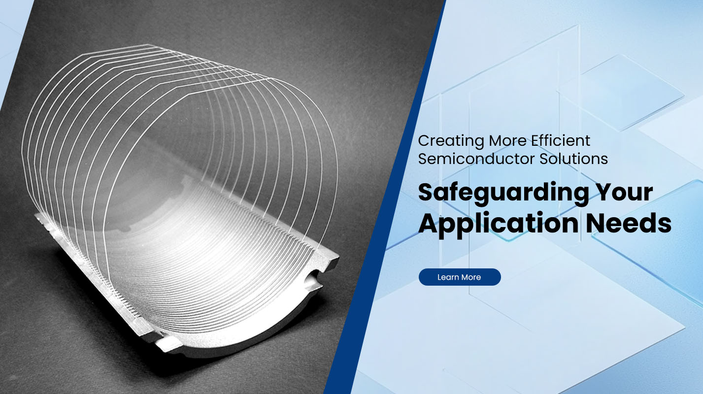
The Process of Creating Silicon Wafers
Silicon Wafers are the backbone of modern electronics, serving as the foundational material for semiconductor devices, solar cells, and various other applications in the tech industry. At PLUTOSEMI, we take pride in producing high-quality silicon wafers, ensuring that each product meets stringent standards for performance and reliability. In this article, we will walk you through the process of creating silicon wafers, from the crystallization of silicon to the final polishing and inspection stages.
1. Silicon Crystal Growth
The process begins with the extraction and purification of silicon. Silicon is derived from sand (silica), which is then purified to remove impurities and contaminants. The purified silicon is melted in a furnace, and a small seed crystal is introduced into the molten silicon. This seed crystal serves as the template for the rest of the silicon to grow around, forming a large cylindrical ingot. This growth process is typically done using the Czochralski method, where the seed crystal is slowly pulled from the molten silicon, allowing the crystal structure to grow and develop.
The resulting silicon ingot, often several feet long, is solid, pure, and free from impurities. This ingot serves as the starting material for creating the silicon wafers.
2. Slicing the Silicon Ingot
Once the silicon ingot has been formed, it needs to be sliced into thin wafers. This step is performed using a process called wire sawing, where a diamond-coated wire is used to slice the ingot into thin disks. The thickness of each wafer is carefully controlled to ensure uniformity and quality.
At PLUTOSEMI, we utilize advanced slicing technology to achieve precise thicknesses for different applications. The wafers can vary in thickness, depending on whether they are intended for use in microelectronics, solar cells, or other high-performance applications.
3. Polishing and Cleaning
After the wafers have been sliced, they undergo a series of polishing and cleaning steps to ensure a smooth, defect-free surface. The wafers are first chemically cleaned to remove any residual impurities or particles left from the slicing process. Following this, the wafers are polished to achieve an ultra-smooth surface, which is crucial for the performance of the final product.
The polishing process helps to remove any microscopic defects on the wafer surface, ensuring that the wafers are ready for the next stage of production, where they will be used in semiconductor manufacturing or other specialized applications.
4. Inspection and Quality Control
At PLUTOSEMI, quality control is a key aspect of our production process. Each wafer is carefully inspected to ensure that it meets the high standards of quality and performance. We use state-of-the-art inspection equipment to detect any defects or imperfections in the silicon wafers, ensuring that only the best products reach our customers.
Our commitment to quality is reflected in our comprehensive testing and inspection protocols, which include checking for surface defects, measuring thickness uniformity, and ensuring the overall integrity of the wafer.
5. Final Product and Application
Once the silicon wafers have been polished, cleaned, and inspected, they are ready for use in a wide range of applications. These include the manufacture of semiconductors, solar cells, microelectronics, and many other high-tech products. The versatility of silicon wafers makes them essential to the modern electronics industry, and PLUTOSEMI is proud to be a trusted supplier of top-quality silicon wafers.
In conclusion, the process of creating silicon wafers involves several critical stages, each of which requires advanced technology and precise control. At PLUTOSEMI, we are dedicated to producing high-performance silicon wafers that meet the needs of industries worldwide. By combining cutting-edge technology with a commitment to quality, we ensure that our customers receive the best possible products for their applications.


