


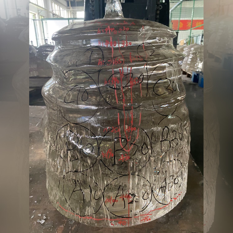
Sapphire Crystal Ingot Block
Sapphire Crystal Ingot

-
+86-17701852595 WhatsApp
-
sales@plutosemitech.com Email
Crystal Ingot Block is a crystal block manufactured based on high-purity materials, with the core being the formation of a single crystal structure through precision controlled growth processes. This type of crystal block typically has a uniform internal structure and is one of the fundamental materials in high-end semiconductor and optoelectronic fields. As an important form of crystal material, Crystal Ingot Block needs to undergo strict quality testing during the production process to ensure high standard requirements for subsequent processing. It is not only the cornerstone of modern industrial technology development, but also a key raw material for achieving high-performance electronic devices and optical components. Its shape is usually a regular geometric shape, which facilitates subsequent cutting, grinding, and polishing processes.

Sapphire Crystal Ingot Block Features
1. High purity and defect free characteristics:
The core advantage of Sapphire Crystal Ingot Block lies in its extremely high purity and defect free internal structure. By adopting advanced crystal growth techniques such as Czochralski's method or Kyropoulos method, this product can achieve a nearly perfect single crystal structure without bubbles, cracks, or other microscopic defects inside. This high-purity characteristic enables it to exhibit excellent performance in subsequent processing, especially in application scenarios that require high precision and stability.
2. Multiple size specifications:
To meet the needs of different customers, Sapphire Crystal Ingot Block offers a variety of size specifications, including 2-inch, 4-inch, and 6-inch crystal ingots. These size specifications cover most of the current mainstream LED substrate market demand, while also supporting customized services to adapt to specific application scenarios. Whether it's small-scale experiments or large-scale production, Plutosemi can provide suitable solutions.
3. Excellent optical performance:
Sapphire Crystal Ingot Block has excellent optical performance, with extremely high transparency and no color difference. This characteristic is due to strict control during the crystal growth process, ensuring the optical uniformity of the material. In addition, sapphire crystal itself has a wide bandgap characteristic, which can maintain good transparency in the ultraviolet to infrared wavelength range, providing an ideal basic material for the design and manufacturing of optical devices.
4. Mechanical strength and high temperature resistance:
As a hard material, Sapphire Crystal Ingot Block has extremely high mechanical strength and wear resistance, with its hardness second only to diamond. At the same time, sapphire crystals also exhibit excellent high-temperature resistance and can maintain stable physical and chemical properties in extreme environments. This makes it an ideal choice for scenarios that require high thermal loads or strong mechanical stresses.
5. Chemical stability and corrosion resistance:
Sapphire Crystal Ingot Block exhibits strong corrosion resistance to most chemicals and remains stable even in strong acid or alkali environments. This chemical stability not only extends the service life of the material, but also makes it widely applicable in harsh environments.
6. Customizable shape and size:
In addition to standard specifications, Plutosemi also offers customized Sapphire Crystal Ingot Block services in various shapes and sizes. Whether it is a square block or other special shapes, flexible design and production can be carried out according to customer needs. This highly customized service capability further enhances the market competitiveness of the product.
7. Quality stability and global recognition:
Plutosemi's Sapphire Crystal Ingot Block has been certified by multiple mainstream LED substrate processing companies both domestically and internationally, and has become one of its core suppliers. Every product undergoes a strict quality inspection process to ensure that every step from raw materials to finished products meets international standards. This quality stability provides customers with reliable assurance.
Sapphire Crystal Ingot Block Process Flow
1. Raw material preparation:
The first step in producing Sapphire Crystal Ingot Block is to select high-purity aluminum oxide (Al₂O₃) as raw material. These raw materials need to undergo rigorous purification to remove any impurities that may affect the quality of the crystal. Only aluminum oxide with a purity of more than 99.99% can enter the next stage.
2. Crystal growth technology:
The core production link of Sapphire Crystal Ingot Block is crystal growth, usually using the Czochralski method or the Kyropoulos method. In this process, aluminum oxide powder is heated to a molten state and then slowly crystallized through a precisely controlled cooling rate to form a single crystal structure. The entire process needs to be carried out in a dust-free environment to avoid external contamination.
3. Temperature and environmental control:
The stability of temperature and environment is crucial during the crystal growth process. Plutosemi uses advanced temperature control systems and inert gas protection devices to ensure that the molten liquid is under constant temperature and pressure conditions. This fine control can effectively prevent bubbles or cracks from appearing inside the crystal.
4. Crystal annealing:
In order to eliminate the residual stress inside the crystal, the Sapphire Crystal Ingot Block needs to be annealed after the growth is completed. This process releases the thermal stress inside the crystal by gradually reducing the temperature, thereby improving the overall mechanical properties of the material.
5. Cutting and shaping:
After the crystal growth is completed, the original crystal ingot will be cut and shaped according to customer needs. Plutosemi is equipped with high-precision cutting equipment that can process the crystal ingot into blocks or sheets of various specifications while ensuring a smooth and flawless surface.
6. Quality inspection:
Each Sapphire Crystal Ingot Block needs to undergo multiple quality inspections before leaving the factory, including optical performance tests, mechanical strength tests, and chemical stability assessments. Only products that fully meet the standards will be delivered to customers.
7. Packaging and transportation:
Finally, the finished product will be properly packaged to prevent damage during transportation. Plutosemi uses professional shock-proof and moisture-proof packaging solutions to ensure that the product arrives safely in the hands of customers.
Sapphire Crystal Ingot Block Application
1. LED Substrate:
Sapphire Crystal Ingot Block is the core material for manufacturing LED substrates, especially for producing high-brightness blue and white LEDs. Due to its excellent optical properties and thermal conductivity, sapphire substrates can significantly improve the luminous efficiency and life of LEDs. At present, Plutosemi's products have been widely used in mainstream LED manufacturing companies at home and abroad.
2. Optical Windows and Lenses:
Sapphire crystals are often used as optical windows and lens materials due to their high transparency and wear resistance. For example, in the aerospace field, optical windows made of sapphire can withstand extreme environmental conditions while maintaining clear imaging effects. In addition, in the field of consumer electronics, sapphire lenses have gradually become the preferred material for high-end mobile phone cameras.
3. Lasers and Sensors:
Sapphire Crystal Ingot Block also plays an important role in the manufacture of lasers and sensors. Its wide bandgap characteristics and high thermal conductivity make it an ideal substrate material for high-performance lasers. In addition, sapphire crystals are also widely used in pressure sensors and temperature sensors.
4. Watch mirrors and protective screens:
Sapphire crystals are widely used in high-end watch mirrors and smartphone screen protectors due to their high hardness and scratch resistance. This material is not only beautiful and durable, but also effectively prevents scratches and damage in daily use.
5. Medical equipment:
In the medical field, Sapphire Crystal Ingot Block is often used to manufacture endoscope windows, surgical instruments and other precision instrument parts. Its biocompatibility and chemical stability make it an ideal choice for the medical industry.
6. Scientific research and laboratory use:
For scientific research institutions and laboratories, Sapphire Crystal Ingot Block is an important tool for researching new materials and developing new technologies. Its high purity and consistency provide reliable guarantee for the accuracy of experimental data.
Packaging and Transportation
The packaging should be able to withstand the impact, vibration, stacking and extrusion that may be encountered during transportation, while also it has to easy to load, unload and handle.
We use professional wafer box packaging. The wafer box is protected by a double layer bag, the inside is a PE bag that can be dust-proof, and the outside is a aluminum foil bag that can be isolated from the air. The two-layer bags are vacuum-packed.
We will choose carton models according to different sizes of products. And between the product and the carton filled with shock-proof EPE foam, play a comprehensive protection.
Finally choose air transport to reach the customer's hands. This allows customers in any country and region to receive the product in the fastest time.
We comply with the Material Safety Data Sheet (MSDS) rules to ensure that the products transported are free of harmful substances and will not cause environmental pollution and explosion and other possible hazards.

Enterprise Strength
Factory Area: 3000 sq
Process:
1. Shaping→2. Edge Profile→3. Lapping→4. Polishing→5. Cleaning→6. Packing→7. Transportation
Capacity:
Glass Wafer --- 30K pcs
Silicon Wafer --- 20K pcs
(Equal to 6in)

Quality Assurance
Quality inspection method: Product inspection in accordance with SEMI standard or according to customer's requirements, together with product COA.
Warranty period: In accordance with the contract requirements.
Quality system management:
●Organize production according to ISO9001 and other quality system standards.
Quality management system and measures:
●Establish a strict quality assurance system, the heads of all departments and quality engineers to ensure the coordinated operation of the quality system.
●Strengthen the quality inspection system, strengthen the process quality control
●Strict material quality control, ensure that the input materials meet the design requirements and technical specifications.
●Implement a timely filing system for technical data to ensure that all processing technical data is complete/accurate.
Quality control in the production stage:
●Production preparation stage: carefully organize relevant personnel to learn product drawings and technical rules, and improve the technical level of employees.
●Quality control of the production process: the implementation of a strict handover system, the previous step of the process to the next step of the transfer, should be detailed processing. At the same time, strengthen the quality inspection system to ensure the quality of each step of the process.
●Quality acceptance: All processes must be quality acceptance before proceeding to the next process.

Pre-sales and After-sales
Pre-sales Service
Professional technical support and commercial team to help you determine product specifications according to product use, and issue specifications.
On-purchase Service
Produce products according to the confirmed specifications and our process.
After Sale Service
We will respond to any product problems encountered by customers or process problems encountered by customers within 24 hours. We can choose from various forms of service, such as email, video conference and so on.
Plutosemi Co., Ltd. was established in 2019, headquartered in Nanhai, Foshan, focusing on the research and development, production, and sales of high-performance semiconductor materials.
Advanced production capacity: We have three major production bases in China, with a monthly production capacity of 100000 equivalent 6-inch silicon wafers and 30000 equivalent 8-inch glass wafers, ensuring stable and efficient product supply for our customers.
High quality products: We provide efficient and stable product supply innovative solutions in the fields of glass wafers, silicon polishing wafers, epitaxial wafers (EPI), silicon on insulator wafers (SOI), and more. Our silicon wafers have the characteristics of ultra-thin, ultraflat, and high-precision, which can meet the needs of various high-end applications. Our glass and quartz substrates are also renowned for their high smoothness and precise aperture design.


