


Single Crystal Sapphire Wafer
Sapphire Wafers

-
+86-17701852595 WhatsApp
-
sales@plutosemitech.com Email
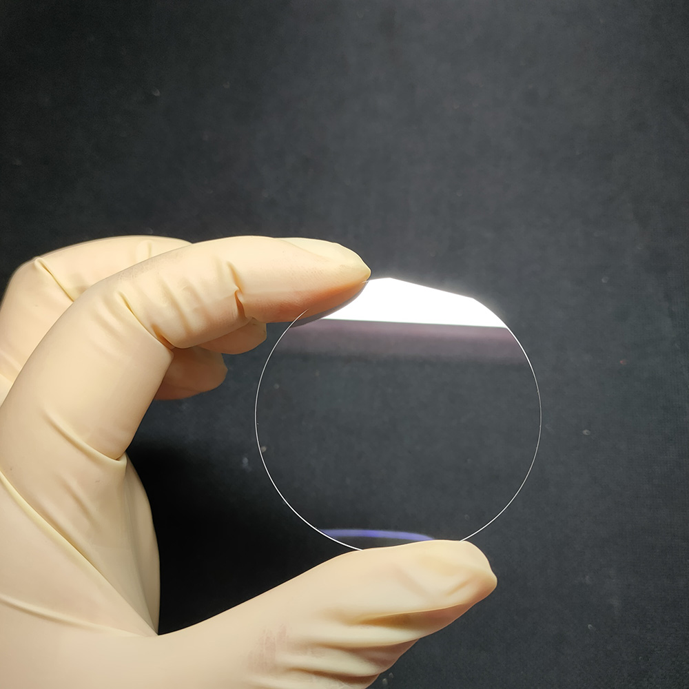
Single Crystal Sapphire Wafer is a single crystal material composed of alumina (Al2O3), which has been widely used in various fields due to its excellent physical and chemical properties. This material is known for its high transparency, high hardness, and excellent thermal stability, making it an ideal choice for manufacturing high-precision optical and electronic components. The manufacturing process of Single Crystal Sapphire Wafer involves precise crystal growth technology, ensuring the uniformity and consistency of the material. The crystal structure of this material is hexagonal, with specific crystal plane orientations such as C-plane (0001), A-plane (11-20), M-plane (10-10), and R-plane (1-102), which are crucial for the final application of the material.

Single Crystal Sapphire Wafer Specifications
Products Standard:
| Product Name | Orientation | Standard Size | Thickness | Polishing |
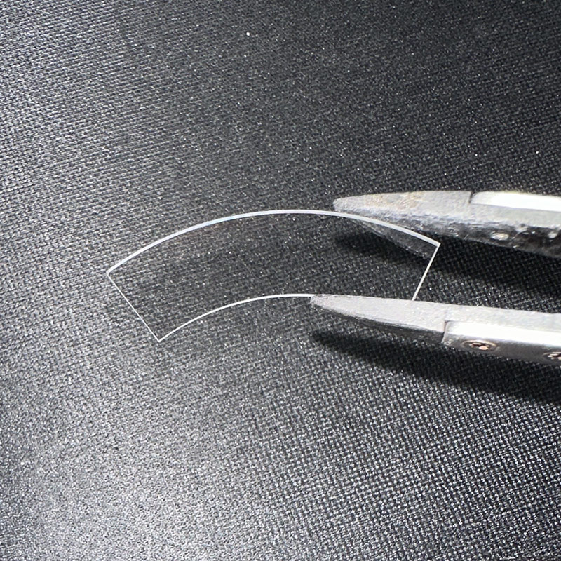
| Sapphire substrate Sapphire wafer | < 0001> ±0.3° < 11-20 > ±0.3° < 10-10 > ±0.3° < 1-102 > ±0.3° Or other off-angle | 10x10mm 10x5mm 5x5mm 20x20mm 100x100mm Φ1" x 0.5mm Φ2" x 0.43mm Φ3" x 0.5mm Φ4" x 0.65mm Φ6" x 1.0mm Φ8" x 1.0mm Or others | 0.1mm 0.2mm 0.5mm 1.0mm 2.0mm Or others | Fine ground Single side polished Double side polished Roughness: Ra < 3A(0.3nm) (Epi-ready) |
Technical Specifications:
| Product Name | Sapphire single crystal substrate, Sapphire wafer, Al2O3 wafer | ||
| Crystal Structure | Hexagonal system | ||
| Orientation | C-plane (0001), A-plane (11-20), M-plane (10-10), R-plane (1-102) | ||
| Lattice Constant | a=4.748Å c=12.97Å | ||
| Density | 3.98(g/cm3) | ||
| Melting Point | 2040℃ | ||
| Mohs Hardness | 9 | ||
| Coefficient of Thermal expansion | 7.5 (x10-6/ oC) | ||
| Thermal conductivity | ⊥c | //c | |
| 23℃ | 0.055 | 26℃ 0.060 | |
| 77℃ | 0.04 | 70℃ 0.041 | |
| Dielectric Constant | ~ 9.4 @300K at A axis ~ 11.58@ 300K at C axis | ||
| Packing | Class-100 Clean bag, in class-1000 clean room | ||
| OEM/ODM | Accept | ||
| Compay Nature | China Manufacturers Suppliers Factory | ||
Single Crystal Sapphire Wafer Features
1. Crystal structure and orientation:
Single Crystal Sapphire Wafer adopts a hexagonal crystal structure, which provides unique physical and chemical properties for the material. It supports a variety of crystal orientations, including C-plane (0001), A-plane (11-20), M-plane (10-10) and R-plane (1-102), which are critical to the final application of the material. Different crystal orientations affect the electrical, optical and mechanical properties of the material, enabling it to meet the needs of specific applications. For example, C-plane is often used to grow III-V and II-VI compounds, such as GaN, for blue LEDs and laser diodes.
2. Lattice constant:
The lattice constant is a basic parameter of the crystal structure. For Single Crystal Sapphire Wafer, its lattice constant is a=4.748Å and c=12.97Å. These precise values ensure the stability and consistency of the material, which is critical for the crystal growth and subsequent processing of the material. Precise control of the lattice constant helps achieve high performance and reliability of the material.
3. Density:
Single Crystal Sapphire Wafer has a density of 3.98 g/cm³, which makes the material achieve a good balance between weight and strength. High density helps improve the material's wear resistance and impact resistance, making it perform well in a variety of applications.
4. Melting point:
The melting point is as high as 2040℃, which allows Single Crystal Sapphire Wafer to maintain its structure and performance in high temperature environments. The high melting point makes it suitable for applications in extreme temperature conditions, such as high-temperature furnace windows, thermocouple protection tubes, etc.
5. Mohs hardness:
The Mohs hardness is 9, second only to diamond, which makes Single Crystal Sapphire Wafer extremely wear-resistant and scratch-resistant. High hardness makes it perform well in applications such as wear-resistant coatings, bearings, and seals.
6. Thermal expansion coefficient:
The thermal expansion coefficient is 7.5 × 10^-6/°C, which helps the material maintain dimensional stability when the temperature changes. Low coefficient of thermal expansion helps reduce deformation and stress caused by temperature changes, and improves the reliability and durability of the material.
7. Thermal conductivity:
The thermal conductivity at different temperatures is 0.055 W/(cm·K) at 23℃ and 0.04 W/(cm·K) at 77℃, which indicates that the material has good thermal management capabilities. High thermal conductivity helps improve the heat dissipation efficiency of electronic devices, reduce operating temperatures, and improve performance and life.
8. Dielectric constant:
At 300K, the dielectric constant of the A axis is about 9.4 and the C axis is about 11.5, which are particularly important for electronic applications. Stable dielectric constants help improve the performance and reliability of electronic devices, especially in high-frequency and high-power applications.
9. Surface roughness:
The surface roughness Ra<3å>
10. Polishing:
Provide fine grinding, single-sided polishing, double-sided polishing and other polishing treatments to meet different application requirements. Different polishing treatments can meet different surface requirements from rough to fine, and improve the applicability and performance of the material.
Single Crystal Sapphire Wafer Process Flow
1. Crystal growth:
The production of Single Crystal Sapphire Wafer first requires crystal growth. Crystal growth is a key step before manufacturing wafers and chips, and single silicon crystals must be extracted. There are two methods for producing single crystal silicon from electronic-grade silicon: the CZOCHRALSKI method (direct pull method) and the floating zone method. The CZOCHRALSKI method melts silicon crystals in a container with a rotating crucible. When there is enough molten silicon, technicians will throw a small ingot into the mixture, and then the molten silicon container will rotate in the opposite direction of the crucible to pull out the silicon rod, which will then be cut into wafers.
2. Wafer cutting:
The rod body produced by the growth process, that is, the silicon rod or silicon ingot, is obtained. After the silicon rod is obtained, it is cut off and trimmed using an electroplated diamond band saw or an inner circle cutting blade according to different product requirements. The inner circle or outer circle cutting efficiency is low, the material loss rate is large, and the processing quality is low, so diamond band saws are currently used to cut silicon rods. The surface of the silicon rod with rounded corners cut off is not a regular cylindrical shape, and the silicon rod needs to be rounded using an electroplated or sintered diamond cup wheel to achieve the required diameter.
3. Grinding:
During grinding, the silicon wafer is fixed on a carrier between the upper and lower grinding discs. When the upper and lower grinding discs rotate in relative directions, the two sides of the silicon wafer can be ground simultaneously. This step is to ensure the thickness and surface flatness of the wafer, laying the foundation for the subsequent polishing steps.
4. Polishing:
After this, it is a wet chemical mechanical polishing (CMP) process, the purpose of which is to achieve a high reflectivity surface on one side of the semiconductor wafer without scratches and damage. The chemical etching process involves using a solution made of hydrofluoric acid (HF) mixed with nitric acid and acetic acid to dissolve silicon. During the CMP process, the wafers are mounted on a fixture and placed in a CMP machine, where they undergo a process that combines chemical and mechanical polishing.
5. Cleaning:
The polished wafers need to be thoroughly cleaned to remove the polishing liquid and other impurities remaining on the surface. This step is critical to ensure the purity of the wafer and is usually completed using ultrasonic cleaning technology combined with appropriate chemical solvents.
6. Inspection:
Use high-precision inspection equipment to inspect the size, shape, surface roughness, etc. of the wafer to ensure product quality. This step is a key link in quality control to ensure that each wafer meets high standards.
7. Packaging:
The qualified wafers are vacuum packed to prevent contamination during transportation and storage. The packaging materials need to have good moisture and dust resistance to ensure that the wafers are in the best condition before they reach the customer.
8. Quality Control:
Throughout the production process, strict quality control measures are implemented to ensure that each wafer meets high standards. This includes comprehensive inspection and evaluation of raw materials, production processes and final products.
9. Customized services:
Customized wafer size, thickness and polishing are provided according to the special needs of customers. This requires a certain degree of flexibility in the production process to adapt to the needs of different customers.
10. Continuous improvement:
Continuously optimize the production process, improve production efficiency and product quality to meet market needs. This involves the continuous updating and upgrading of production equipment, process flows and operating techniques.
Single Crystal Sapphire Wafer Application
1. Optical windows:
Single Crystal Sapphire Wafer is widely used as high-temperature infrared windows and protective covers due to its high transparency and wear resistance. This material can withstand extreme temperatures and environmental conditions while maintaining its optical properties, making it an ideal choice for military and industrial applications. For example, it can be used for infrared windows of ground-to-ground and ground-to-air missiles, as well as windows for high-temperature pressure-sensitive sensors.
2. Electronic devices:
In the semiconductor industry, Sapphire Wafer is used as a substrate material, especially in the manufacture of LEDs and lasers. Sapphire single crystal is an excellent multifunctional material that can be widely used in many fields such as industry, defense and scientific research (such as high-temperature resistant infrared windows). Generally speaking, C-face (0001) sapphire is used in this field. R-face (1-102) or M (10-10) face is mainly used to grow non-polar/semi-polar planar epitaxial layers to improve luminescence efficiency.
3. Wear-resistant coating:
Due to its high hardness, Single Crystal Sapphire Wafer can be used to make wear-resistant coatings for watch mirrors, mobile phone screens, etc. The hardness of this material is second only to diamond, with a Mohs hardness of 9, which makes it excellent in wear-resistant coating applications and can provide long-term protection and durability.
4. Sensors:
In pressure sensors and temperature sensors, Sapphire Wafer is widely used due to its stability and corrosion resistance. Sapphire substrate has the characteristics of stable dielectric constant and low dielectric loss, and is the most commonly used substrate for HIC and the main substrate for MCM. These characteristics enable Sapphire Wafer to provide high precision and reliability in sensor applications.
5. Optical components:
In optical instruments, Sapphire Wafer is used to make lenses, prisms and other optical components due to its high refractive index and low dispersion. The optical properties of this material make it perform well in applications such as optical windows, lenses and prisms, helping to improve optical performance and image quality.
6. Wear-resistant parts:
In industrial machinery, Sapphire Wafer is used as wear-resistant parts such as bearings and seals. The high hardness and wear resistance of this material make it very popular in these applications, providing long-term durability and performance.
7. Scientific instruments:
In the field of scientific research, Sapphire Wafer is used to manufacture high-precision scientific instruments such as spectrometers and microscopes. The stability and precision of this material make it play a key role in scientific instruments, helping to improve the accuracy and reliability of experimental results.
8. Aerospace:
In the field of aerospace, Sapphire Wafer is used to manufacture parts that are resistant to high temperatures and pressures, such as those of jet engines. The high temperature and high pressure resistance of this material makes it very important in aerospace applications and can withstand extreme working environments.
9. Medical devices:
In medical devices, Sapphire Wafer is used to manufacture scalpels and other medical devices due to its biocompatibility and corrosion resistance. The biocompatibility of this material makes it very useful in medical devices, providing safe and effective medical solutions.
10. Jewelry Industry:
In the jewelry industry, Sapphire Wafer is used to make fine jewelry because of its beauty and durability. The beauty and durability of this material makes it very popular in the jewelry industry, enabling the creation of jewelry products that are both beautiful and durable.
Packaging and Transportation
The packaging should be able to withstand the impact, vibration, stacking and extrusion that may be encountered during transportation, while also it has to easy to load, unload and handle.
We use professional wafer box packaging. The wafer box is protected by a double layer bag, the inside is a PE bag that can be dust-proof, and the outside is a aluminum foil bag that can be isolated from the air. The two-layer bags are vacuum-packed.
We will choose carton models according to different sizes of products. And between the product and the carton filled with shock-proof EPE foam, play a comprehensive protection.
Finally choose air transport to reach the customer's hands. This allows customers in any country and region to receive the product in the fastest time.
We comply with the Material Safety Data Sheet (MSDS) rules to ensure that the products transported are free of harmful substances and will not cause environmental pollution and explosion and other possible hazards.

Enterprise Strength
Factory Area: 3000 sq
Process:
1. Shaping→2. Edge Profile→3. Lapping→4. Polishing→5. Cleaning→6. Packing→7. Transportation
Capacity:
Glass Wafer --- 30K pcs
Silicon Wafer --- 20K pcs
(Equal to 6in)

Quality Assurance
Quality inspection method: Product inspection in accordance with SEMI standard or according to customer's requirements, together with product COA.
Warranty period: In accordance with the contract requirements.
Quality system management:
●Organize production according to ISO9001 and other quality system standards.
Quality management system and measures:
●Establish a strict quality assurance system, the heads of all departments and quality engineers to ensure the coordinated operation of the quality system.
●Strengthen the quality inspection system, strengthen the process quality control
●Strict material quality control, ensure that the input materials meet the design requirements and technical specifications.
●Implement a timely filing system for technical data to ensure that all processing technical data is complete/accurate.
Quality control in the production stage:
●Production preparation stage: carefully organize relevant personnel to learn product drawings and technical rules, and improve the technical level of employees.
●Quality control of the production process: the implementation of a strict handover system, the previous step of the process to the next step of the transfer, should be detailed processing. At the same time, strengthen the quality inspection system to ensure the quality of each step of the process.
●Quality acceptance: All processes must be quality acceptance before proceeding to the next process.

Pre-sales and After-sales
Pre-sales Service
Professional technical support and commercial team to help you determine product specifications according to product use, and issue specifications.
On-purchase Service
Produce products according to the confirmed specifications and our process.
After Sale Service
We will respond to any product problems encountered by customers or process problems encountered by customers within 24 hours. We can choose from various forms of service, such as email, video conference and so on.
Plutosemi Co., Ltd. was established in 2019, headquartered in Nanhai, Foshan, focusing on the research and development, production, and sales of high-performance semiconductor materials.
Advanced production capacity: We have three major production bases in China, with a monthly production capacity of 100000 equivalent 6-inch silicon wafers and 30000 equivalent 8-inch glass wafers, ensuring stable and efficient product supply for our customers.
High quality products: We provide efficient and stable product supply innovative solutions in the fields of glass wafers, silicon polishing wafers, epitaxial wafers (EPI), silicon on insulator wafers (SOI), and more. Our silicon wafers have the characteristics of ultra-thin, ultraflat, and high-precision, which can meet the needs of various high-end applications. Our glass and quartz substrates are also renowned for their high smoothness and precise aperture design.


