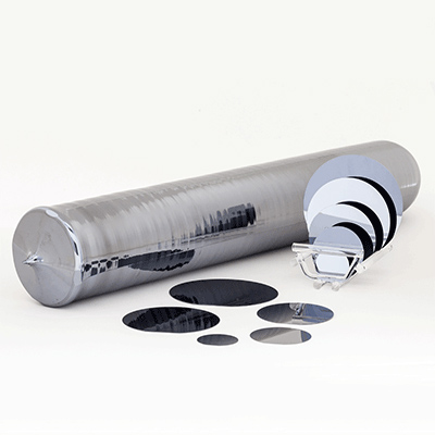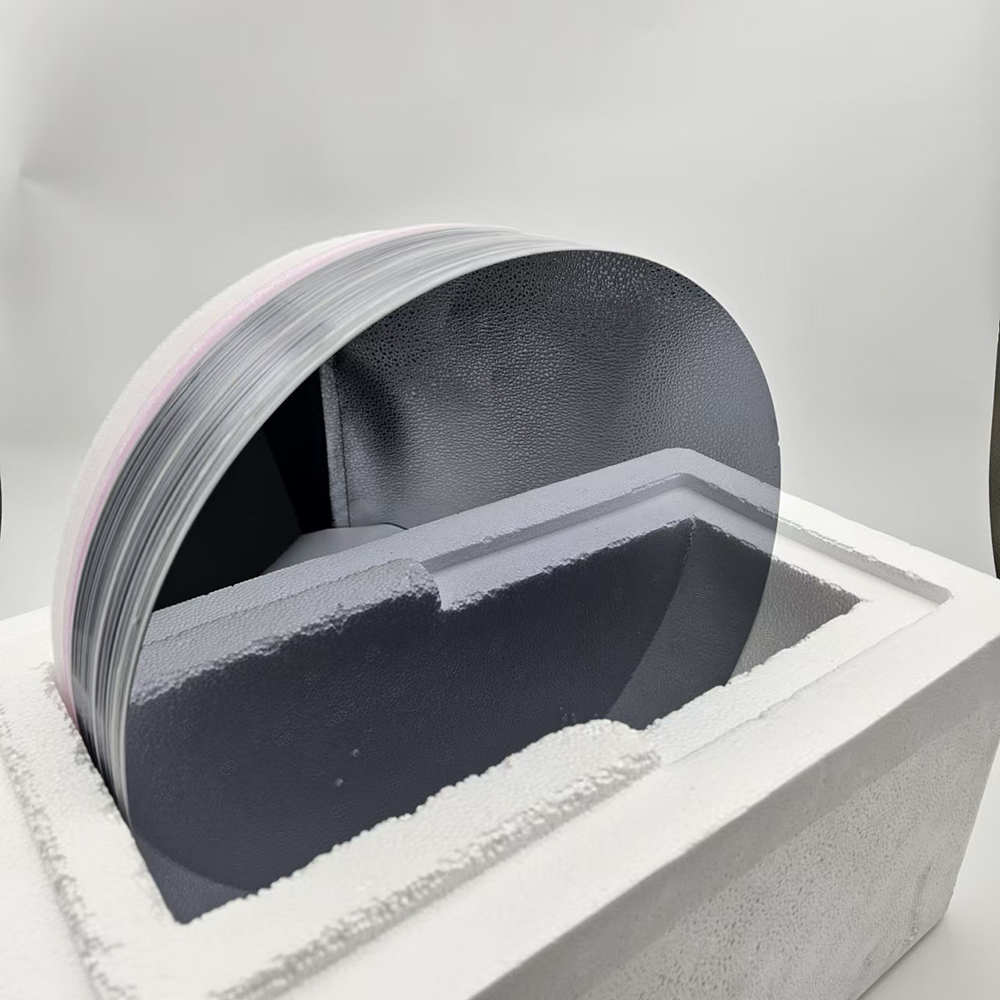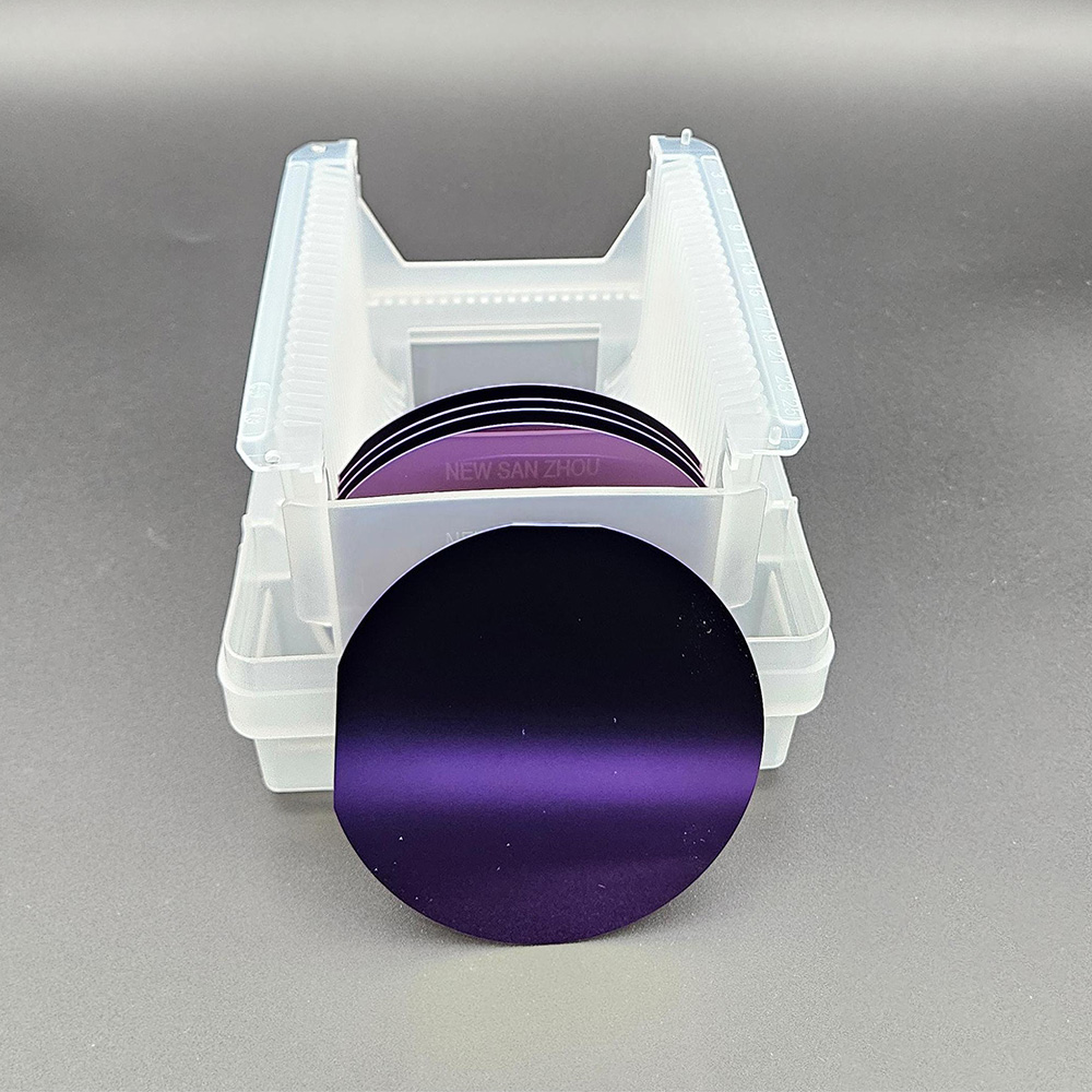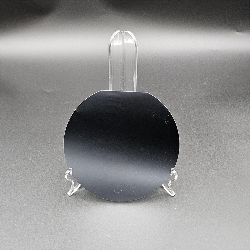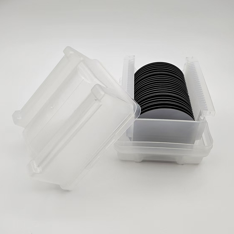
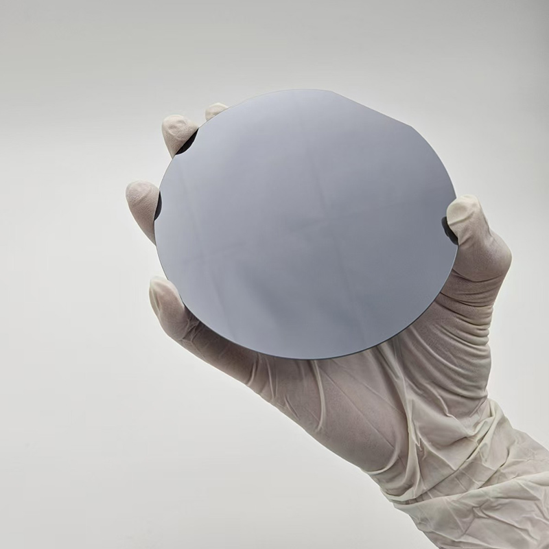
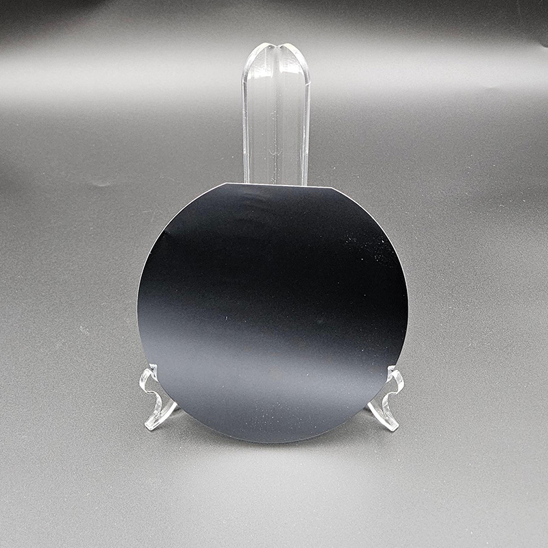
Float Zone Silicon Wafer
Silicon Wafer

-
+86-17701852595 WhatsApp
-
sales@plutosemitech.com Email
Float Zone Silicon Wafer is a high-purity silicon material produced by the Float Zone Method. The silicon produced by this method has extremely high purity, so it has a low defect concentration and high resistivity. These characteristics make Float Zone silicon wafers excel in fields such as high-voltage devices, detectors, and solar applications. They are not produced by the CZ remelting method, but use high-quality polycrystalline silicon as raw material, so they can achieve resistivity exceeding 10k ohm cm, which helps reduce current leakage and power consumption.

Float Zone Silicon Wafer Specifications
| Diameter | 2" | 3" | 4" | 5" | 6" | 8" |
| Growth Method | FZ | |||||
| Orientation | < 1-0-0 >, < 1-1-1 > | |||||
| Type/Dopant | Intrinsic,N Type/Phos, P Type/Boron | |||||
| Thickness(μm) | 279 | 380 | 525 | 625 | 675 | 725 |
| Thickness Tolerance | Standard ± 25μm | ±50μm | ||||
| Resistivity(Ω·cm) | 1000-20000, Maximμm Capabilities > 20000, and 1-5 | |||||
| Surface Finished | P/E, P/P, E/E, G/G | |||||
| TTV(μm) | Standard< 10μm | |||||
| Bow/Warp(μm) | Standard< 40μm | < 50μm | ||||
| Particle | < 10@0.3μm | |||||
Float Zone Silicon Wafer Features
1. High purity:
FZ silicon wafers are produced by the floating zone method. In this process, the silicon rod is melted under high-frequency induction heating and pulled down by its own gravity to form a single crystal. No crucible is required in the whole process, thus avoiding the contamination of silicon by crucible materials. Due to this crucible-free melting method, FZ silicon wafers have extremely low impurity content and are generally higher in purity than silicon wafers prepared by other methods. High purity means lower defect concentrations in FZ silicon wafers, which helps improve the electrical performance and reliability of devices and reduce performance degradation caused by impurities.
2. Diverse diameters and specifications:
Those silicon wafers are available in a variety of specifications and sizes, with diameters ranging from 2 inches to 8 inches, which can be customized to meet the needs of different application scenarios. With the continuous development of semiconductor technology, the demand for larger diameter silicon wafers is also increasing, and FZ silicon wafers are constantly adapting to this trend, providing larger wafers to meet market demand.
3. Excellent doping uniformity:
Float Zone Silicon Wafer can achieve very uniform doping during the growth process, because its growth mechanism determines that the distribution of doping elements in silicon crystals is more uniform. Uniform doping helps improve the consistency and performance stability of devices and reduce performance fluctuations caused by uneven doping. Through advanced technologies such as neutron transmutation doping (NTD), the doping uniformity of FZ silicon wafers can be further improved, making its resistivity variation range smaller and meeting higher precision application requirements.
4. Suitable for high-performance devices:
Due to the high purity and high resistivity of Float Zone Silicon Wafer, it is particularly suitable for manufacturing high-power semiconductor devices, ultra-high frequency devices (such as RF and microwave transistors), high-voltage switches, power rectifiers, and photodetectors.
Float Zone Silicon Wafer Application
1. Power semiconductor devices:
Due to its high resistivity and low defect concentration, it is particularly suitable for manufacturing high-voltage and high-power semiconductor devices, such as insulated gate bipolar transistors (IGBTs), thyristors, silicon-controlled rectifiers (SCRs), etc. These devices play an important role in power electronic systems and are used to control, convert and regulate electrical energy.
2. Photo sensors and other sensors:
The high purity of Float Zone Silicon Wafer reduces the impact of impurities on the absorption and scattering of light signals, and improves the sensitivity and accuracy of photo sensors. Therefore, it is widely used in the manufacture of optoelectronic devices such as photo sensors, photodiodes, and photocouplers.
3. High-frequency and radio-frequency devices:
It also has excellent electrical properties and is suitable for the manufacture of high-frequency and radio-frequency devices, such as radio-frequency transistors, microwave integrated circuits, etc. These devices are widely used in communications, radar, satellite navigation and other fields.
4. Terahertz optical components:
Float Zone Silicon Wafers have high permeability to terahertz radiation, so they are often used to manufacture optical components that require high permeability to terahertz radiation, such as lenses and windows. These components play an important role in terahertz imaging, terahertz spectroscopy and other fields.
5. Detectors:
Its high purity and low defect concentration make it an ideal material for making highly sensitive detectors. These detectors are widely used in particle physics, astronomy, environmental monitoring and other fields to detect weak signals or specific particles.
6. Solar energy applications:
Despite its high production cost, its high purity and excellent electrical properties still make it an attractive material choice in some high-end solar energy applications, such as space solar power stations, high-efficiency solar cells, etc.
Plutosemi Co., Ltd. was established in 2019, headquartered in Nanhai, Foshan, focusing on the research and development, production, and sales of high-performance semiconductor materials.
Advanced production capacity: We have three major production bases in China, with a monthly production capacity of 100000 equivalent 6-inch silicon wafers and 30000 equivalent 8-inch glass wafers, ensuring stable and efficient product supply for our customers.
High quality products: We provide efficient and stable product supply innovative solutions in the fields of glass wafers, silicon polishing wafers, epitaxial wafers (EPI), silicon on insulator wafers (SOI), and more. Our silicon wafers have the characteristics of ultra-thin, ultraflat, and high-precision, which can meet the needs of various high-end applications. Our glass and quartz substrates are also renowned for their high smoothness and precise aperture design.