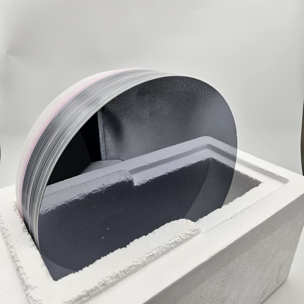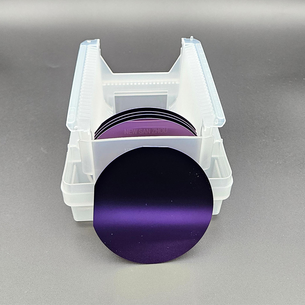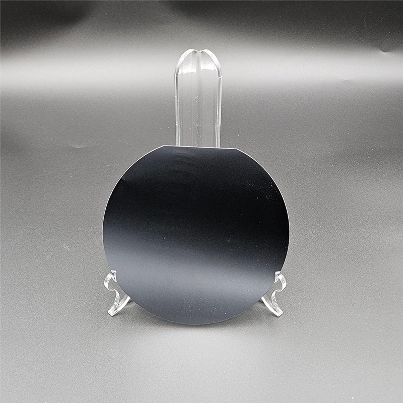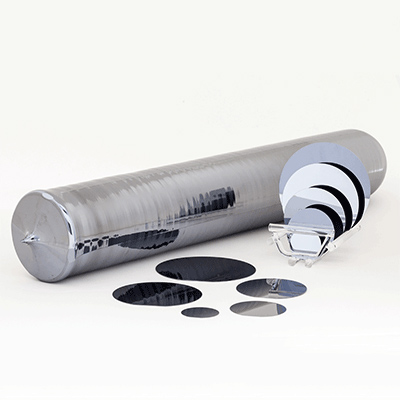
Float Zone Wafer
Silicon Wafer

-
+86-17701852595 WhatsApp
-
sales@plutosemitech.com Email
Float Zone Wafer is a high-purity silicon wafer prepared by the Float Zone Method. Floating zone method is an advanced crystal growth technique that locally melts polycrystalline silicon rods at high temperatures and uses surface tension to move the melted area along the rod body, thereby forming single crystal silicon. This process does not require the use of crucibles, avoiding impurity contamination, thus enabling the production of extremely high purity silicon materials. Float Zone Wafer has become an important foundational material for the semiconductor industry and high-tech fields due to its excellent purity and uniformity.


Float Zone Wafer Specifications
| Diameter | 2", 3" , 4" , 5", 6", 8", 12" |
| Grade | Prime |
| Growth Method | FZ (Flow Zone) |
| Orientation | < 1-0-0 > , < 1-1-1 > , < 1-1-0 > |
| Type/Dopant | Intrinsic, Undoped, P Type/Boron , N Type/Phos, NTD, Gas-Doped, |
| Resistivity | > 5000Ω·cm, > 10000Ω·cm, > 20000Ω·cm |
| Life Time | > 500us, > 1000us |
| OEM/ODM | Accept |
| Compay Nature | China Manufacturers Suppliers Factory |


Float Zone Wafer Features
1. Low defect concentration
Due to the avoidance of crucible contact and impurity introduction by the floating zone method, float zone silicon wafers have a lower concentration of crystal defects. This characteristic makes it perform well in high-precision electronic devices, especially in applications that require stability and consistency.
2. High resistivity range
The resistivity of float zone silicon wafers can reach over 10k ohm cm, much higher than that of ordinary silicon wafers. This high resistivity characteristic makes it very suitable for the manufacturing of high-power devices and precision detectors.
3. Excellent uniformity
Float Zone Wafer is known for its excellent resistivity uniformity, especially in the Neutron Transmutation Doped (NTD) silicon products, where the range of resistivity variation is extremely small, making it the lowest among any crystalline silicon products on the market.
4. Diversified specification selection
PLUTO offers a wide range of Float Zone Wafer diameters, up to 200mm, and supports multiple customized specifications to meet the needs of different customers.
5. Wide range of resistivity coverage
The resistivity range of NTD Float Zone silicon ranges from 5 Ω• cm to 4000 Ω• cm, covering almost all high-end application needs and providing customers with flexible choices.
6. Environmental Protection and Sustainability
The production process of Float Zone Wafer focuses on environmental protection and reduces its impact on the environment. Its high purity and performance also reduce resource waste, in line with the concept of modern green manufacturing.
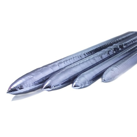
Float Zone Wafer Process Flow
The production of float zone silicon wafers begins with the preparation of high-quality polycrystalline silicon rods. These raw materials have undergone strict screening to ensure their purity and consistency meet the requirements of the floating zone method. In the floating zone method, the polycrystalline silicon rod is locally heated to its melting point, forming a narrow melting zone. By slowly moving the molten region, silicon crystals will gradually grow into a single crystal structure. The unique feature of the floating zone method lies in its crucible free design, which avoids the contamination that may be caused by crucible materials in traditional direct drawing methods, thereby further improving the purity of silicon wafers. By adjusting the type and concentration of dopants, the resistivity of Float Zone Wafer can be precisely controlled to meet the needs of different application scenarios. The grown single crystal silicon rod is cut into thin slices and subjected to precision polishing treatment to obtain a smooth surface and precise thickness. Each Float Zone Wafer undergoes a rigorous testing process, including resistivity measurement, crystal structure analysis, and surface quality inspection, to ensure that the product meets high standards.
Float Zone Wafer Application
1. High power electronic devices
Float Zone Wafer is widely used in the manufacturing of high-power electronic devices, such as power amplifiers, rectifiers, and inverters, due to its high resistivity and low defect concentration.
2. Detectors and sensors
In the field of radiation detectors and high-sensitivity sensors, the high purity and uniformity of float zone silicon wafers make it an indispensable material, particularly suitable for medical imaging equipment and nuclear physics research.
3. Solar cells
Float Zone Wafer is also widely used in high-efficiency solar cells, and its high purity and low defect characteristics can significantly improve the photoelectric conversion efficiency.
4. Research and laboratory applications
Due to its excellent performance, Float Zone Wafer is often used in scientific research and laboratory testing, such as semiconductor material research and the development of new electronic devices.
5. Aerospace and Defense
In the aerospace and defense fields, Float Zone Wafer is used to manufacture high-performance radar systems, communication equipment, and navigation instruments, and its reliability is crucial.
6. Industrial automation
The control system and sensors in industrial automation equipment also rely on the high performance of Float Zone Wafer to ensure the accuracy and stability of equipment operation.
7. Communication technology
In the fields of optical and wireless communication, Float Zone Wafer is used to manufacture high-frequency signal processing chips and optoelectronic devices, improving data transmission speed and quality.
8. New energy technologies
With the development of new energy technologies, the application of Float Zone Wafer in electric vehicle battery management systems and smart grids is increasing, promoting the advancement of clean energy technology.
Plutosemi Co., Ltd. was established in 2019, headquartered in Nanhai, Foshan, focusing on the research and development, production, and sales of high-performance semiconductor materials.
Advanced production capacity: We have three major production bases in China, with a monthly production capacity of 100000 equivalent 6-inch silicon wafers and 30000 equivalent 8-inch glass wafers, ensuring stable and efficient product supply for our customers.
High quality products: We provide efficient and stable product supply innovative solutions in the fields of glass wafers, silicon polishing wafers, epitaxial wafers (EPI), silicon on insulator wafers (SOI), and more. Our silicon wafers have the characteristics of ultra-thin, ultraflat, and high-precision, which can meet the needs of various high-end applications. Our glass and quartz substrates are also renowned for their high smoothness and precise aperture design.