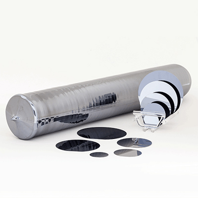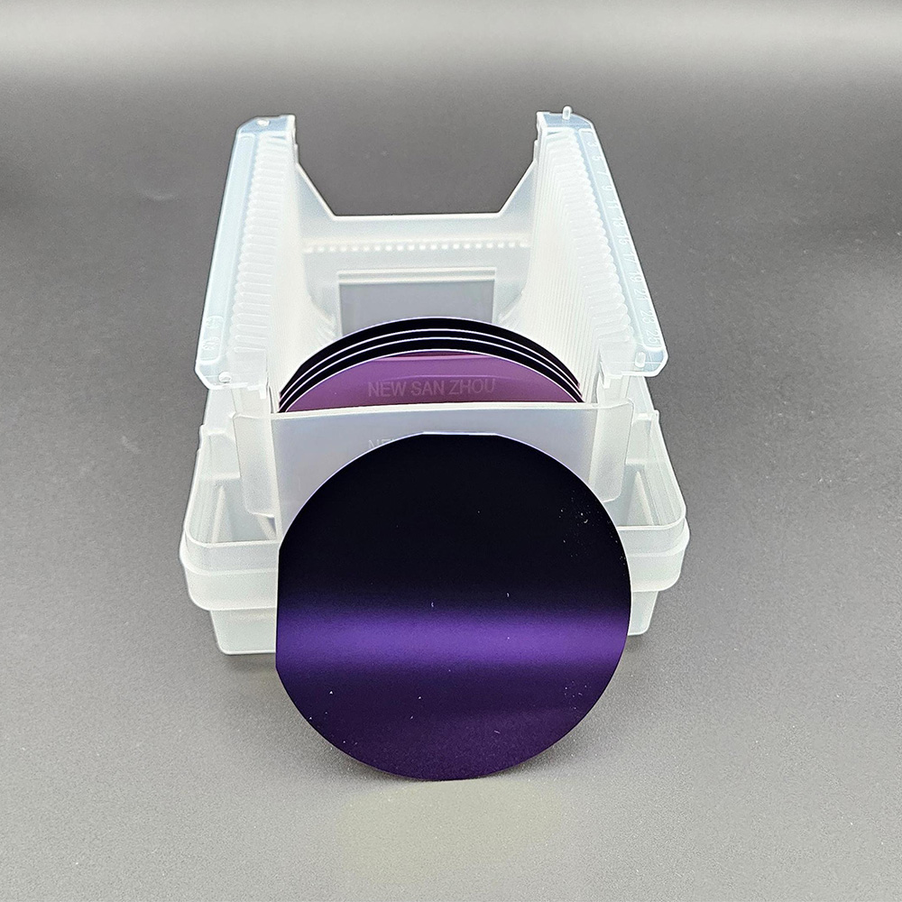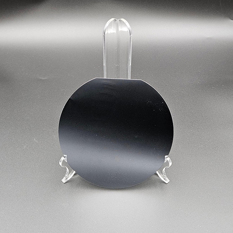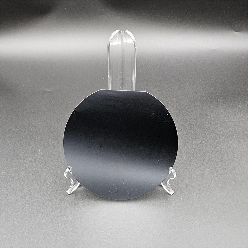
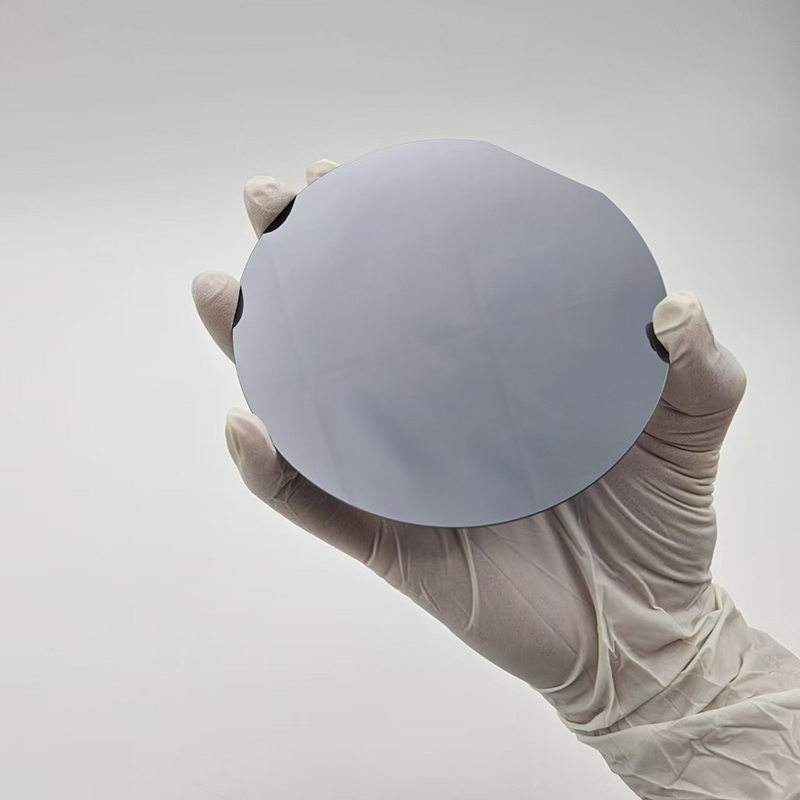
Neutron Transmutation Doping Silicon Wafer
Silicon Wafer

-
+86-17701852595 WhatsApp
-
sales@plutosemitech.com Email
NTD Silicon Wafer is an innovative technology that achieves semiconductor doping through nuclear reactions. Its core principle is to use neutron bombardment of high-purity silicon wafers to trigger isotope transformation reactions, generating donor impurities (such as phosphorus), and directly forming N-type semiconductors. NTD technology breaks through the physical limitations of traditional doping and provides a new dimension for semiconductor processing, especially in scenarios that require deep junctions, high uniformity, or low-temperature processes, with unique advantages.

Neutron Transmutation Doping Silicon Wafer Specifications
| Diameter | 2" | 3" | 4" | 5" | 6" | 8" | 12" |
| Grade | Prime | ||||||
| Growth Method | NTD | ||||||
| Orientation | < 1-0-0 >,< 1-1-1 >,< 1-1-0 > | ||||||
| Type/Dopant | N Type/Phos | ||||||
| Thickness(um) | 279 | 380 | 525 | 625 | 675 | 725 | 775 |
| Thickness Tolerance | Standard ±25μm, Maximum Capabilities ±5μm | ±20μm | ±20μm | ||||
| Resistivity | > 100 ohm-cm | ||||||
| Surface Finished | P/E, P/P, E/E, G/G | ||||||
| TTV(um) | Standard<10um, maximum="" capabilities=""> | ||||||
| Bow/Warp(um) | Standard<40um, maximum="" capabilities=""> | < 40μm | < 40μm | ||||
| Particle | <10@0.5um;> | ||||||
Neutron Transmutation Doping Silicon Wafer Features
1. Accurate doping control
Neutron dose control: By adjusting the neutron flux (number of neutrons per unit area) and irradiation time, the doping concentration of phosphorus or boron can be precisely controlled. For example, when the neutron flux in a reactor reaches 10 ¹³ cm ⁻² · s ⁻¹, there is a linear relationship between doping concentration and irradiation time. Low temperature (such as room temperature) irradiation can reduce the influence of thermal diffusion and achieve steep doping gradients; High temperature annealing (such as 800 ℃) can activate impurities and repair lattice damage, optimizing electrical properties. Neutrons can penetrate the entire wafer to prepare uniformly doped layers or achieve selective doping by combining mask technology.
2. Low impurity doping
Optimization of concentration range: 10 ¹⁵ cm ⁻ ³ (ultra-low doping) is suitable for high resistance sensors, and 10 ¹⁸ cm ⁻ ³ (medium doping) is suitable for power devices. For example, doping with 10 ¹⁶ cm ⁻ ³ phosphorus can achieve N-type silicon of 0.1 Ω· cm, balancing conductivity and breakdown voltage. Compared with traditional diffusion methods, the standard deviation of impurity distribution in NTD is reduced by 50%, reducing local electric field concentration and improving device reliability.
3. High temperature stability
Advantages of thermal activation energy: The binding energy between phosphorus and silicon lattice generated by neutron transmutation (about 0.45 eV) is higher than that after ion implantation damage, and the impurity diffusion coefficient is reduced by two orders of magnitude at high temperatures (>300 ℃).
4. High purity materials
Preparation process: Single crystal silicon is grown using suspension zone melting (FZ) method with impurity concentration<10 ¹² cm ⁻ ³, and surface roughness<0.2 nm is achieved by combining chemical mechanical polishing (CMP). In high-purity silicon, the doping efficiency of NTD is increased by 40%, and the activation rate of impurities is increased from 85% to 98% due to the reduction of intrinsic defects.
5. Crystal integrity
Defect density comparison: The vacancy defect density introduced by NTD is less than 10 ⁸ cm ⁻ ², which is 3 orders of magnitude lower than ion implantation (>10 ¹¹ cm ⁻ ²), and the carrier mobility is increased by 15%. The lifetime of minority carriers has been extended from 1 μ s after ion implantation to 10 μ s for NTD, making it possible for high-efficiency solar cells (>24% efficiency).
Neutron Transmutation Doping Silicon Wafer Application
1. High performance integrated circuits:
NTD silicon wafer has a wide range of applications in high-performance integrated circuits. By precise doping control, transistors and logic gates with high electrical performance can be manufactured. This technology is suitable for manufacturing microprocessors, memory chips, and other complex integrated circuits, ensuring their advantages in high-performance computing and data storage.
2. High voltage devices:
Neutron Transmutation Doping Silicon Wafer can be applied to high-voltage devices such as high-voltage transistors and high-voltage diodes. By controlling the doping concentration and distribution, high voltage resistance performance can be achieved. This characteristic makes NTD silicon wafers perform well in fields such as automotive electronics and industrial control.
3. Biomedical sensors:
NTD silicon wafers are widely used in biomedical sensors due to their high purity and good biocompatibility. For example, sensitive and stable biosensors can be manufactured using NTD technology for medical diagnosis and biological monitoring.
4. High performance optoelectronic components:
NTD silicon wafer perform well in optoelectronic components such as solar cells and photodiodes. By precisely controlling doping, the photoelectric conversion efficiency can be optimized, the photoelectric performance of the device can be improved, and it is suitable for photovoltaic technology and photodetectors.
5. High temperature environment application:
NTD silicon wafer can maintain stable electrical properties in high temperature environments, making them suitable for high-temperature applications. This characteristic makes NTD silicon wafers have important application value in fields such as automotive electronics, industrial control, and aerospace.
6. Special electronic devices:
NTD silicon wafer can be used to prepare electronic devices with special electrical properties, such as high resistivity resistance devices and low resistivity wires. These special devices can provide unique performance advantages in specific application scenarios, improving the overall performance of the system.
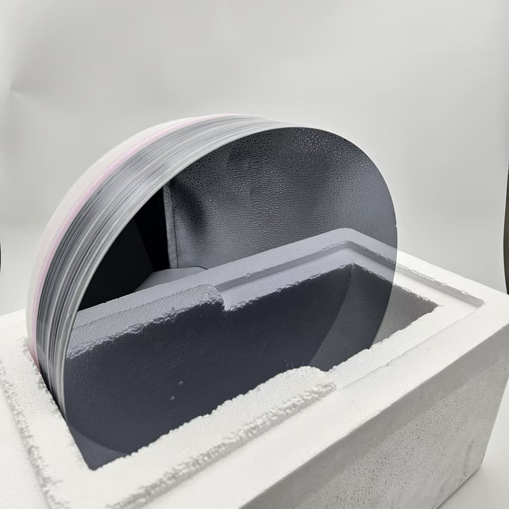
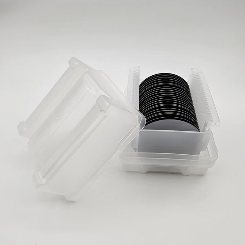
Packaging and Transportation
The packaging should be able to withstand the impact, vibration, stacking and extrusion that may be encountered during transportation, while also it has to easy to load, unload and handle.
We use professional wafer box packaging. The wafer box is protected by a double layer bag, the inside is a PE bag that can be dust-proof, and the outside is a aluminum foil bag that can be isolated from the air. The two-layer bags are vacuum-packed.
We will choose carton models according to different sizes of products. And between the product and the carton filled with shock-proof EPE foam, play a comprehensive protection.
Finally choose air transport to reach the customer's hands. This allows customers in any country and region to receive the product in the fastest time.
We comply with the Material Safety Data Sheet (MSDS) rules to ensure that the products transported are free of harmful substances and will not cause environmental pollution and explosion and other possible hazards.

Enterprise Strength
Factory Area: 3000 sq
Process:
1. Shaping→2. Edge Profile→3. Lapping→4. Polishing→5. Cleaning→6. Packing→7. Transportation
Capacity:
Glass Wafer --- 30K pcs
Silicon Wafer --- 20K pcs
(Equal to 6in)

Quality Assurance
Quality inspection method: Product inspection in accordance with SEMI standard or according to customer's requirements, together with product COA.
Warranty period: In accordance with the contract requirements.
Quality system management:
●Organize production according to ISO9001 and other quality system standards.
Quality management system and measures:
●Establish a strict quality assurance system, the heads of all departments and quality engineers to ensure the coordinated operation of the quality system.
●Strengthen the quality inspection system, strengthen the process quality control
●Strict material quality control, ensure that the input materials meet the design requirements and technical specifications.
●Implement a timely filing system for technical data to ensure that all processing technical data is complete/accurate.
Quality control in the production stage:
●Production preparation stage: carefully organize relevant personnel to learn product drawings and technical rules, and improve the technical level of employees.
●Quality control of the production process: the implementation of a strict handover system, the previous step of the process to the next step of the transfer, should be detailed processing. At the same time, strengthen the quality inspection system to ensure the quality of each step of the process.
●Quality acceptance: All processes must be quality acceptance before proceeding to the next process.

Pre-sales and After-sales
Pre-sales Service
Professional technical support and commercial team to help you determine product specifications according to product use, and issue specifications.
On-purchase Service
Produce products according to the confirmed specifications and our process.
After Sale Service
We will respond to any product problems encountered by customers or process problems encountered by customers within 24 hours. We can choose from various forms of service, such as email, video conference and so on.
Plutosemi Co., Ltd. was established in 2019, headquartered in Nanhai, Foshan, focusing on the research and development, production, and sales of high-performance semiconductor materials.
Advanced production capacity: We have three major production bases in China, with a monthly production capacity of 100000 equivalent 6-inch silicon wafers and 30000 equivalent 8-inch glass wafers, ensuring stable and efficient product supply for our customers.
High quality products: We provide efficient and stable product supply innovative solutions in the fields of glass wafers, silicon polishing wafers, epitaxial wafers (EPI), silicon on insulator wafers (SOI), and more. Our silicon wafers have the characteristics of ultra-thin, ultraflat, and high-precision, which can meet the needs of various high-end applications. Our glass and quartz substrates are also renowned for their high smoothness and precise aperture design.