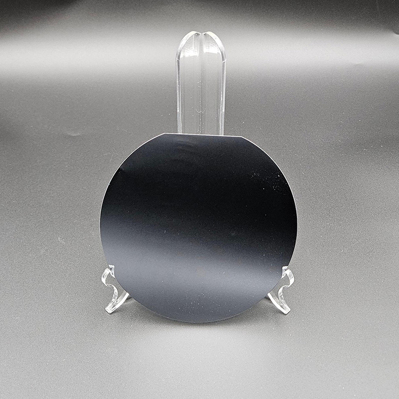
P Type Silicon Wafer
Silicon Wafer

-
+86-17701852595 WhatsApp
-
sales@plutosemitech.com Email
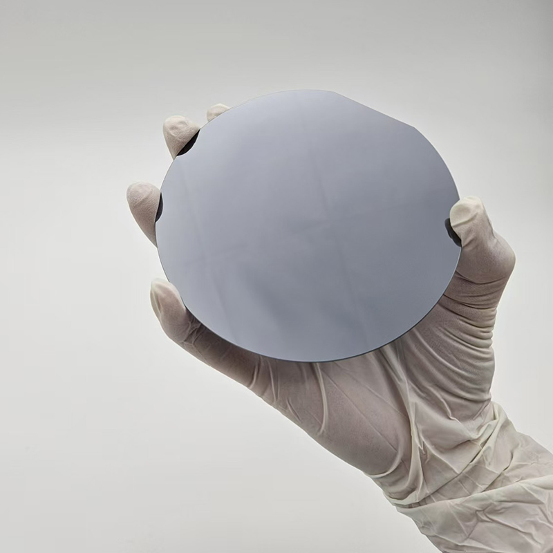
P type silicon wafer is a widely used basic material in the semiconductor industry. It is based on high-purity single crystal silicon and is doped with an appropriate amount of trivalent elements (such as boron) to increase the hole concentration in the silicon material, thereby forming P-type semiconductor characteristics. This doping process can precisely control the conductivity of silicon wafers, enabling them to play a critical role in different electronic devices and applications. The manufacturing process of P-type silicon wafers includes multiple fine steps such as crystal growth, cutting, grinding, polishing, etc., to ensure that they have high flatness, low surface roughness, and precise resistivity, meeting the strict requirements of modern semiconductor manufacturing for materials.

P Type Silicon Wafer Specifications
| Diameter | 2" | 3" | 4" | 5" | 6" | 8" | 12" |
| Grade | Prime Test Dummy | ||||||
| Growth Method | CZ | ||||||
| Orientation | < 1-0-0 >, < 1-1-1 >,< 1-1-0 > | ||||||
| Type/Dopant | Type/Boron, N Type/Phos, N Type/As, N Type/Sb | ||||||
| Thickness(um) | 279 | 380 | 525 | 625 | 675 | 725 | 775 |
| Thickness Tolerance | Standard ±25μm, Maximum Capabilities ±5μm | ±20μm | ±20μm | ||||
| Resistivity | 0.001-100 ohm-cm | ||||||
| Surface Finished | P/E, P/P, E/E, G/G | ||||||
| TTV(um) | Standard < 10um, Maximum Capabilities < 5um | ||||||
| Bow/Warp(um) | Standard < 40um, Maximum Capabilities < 20um | < 40μm | < 40μm | ||||
| Particle | <10@0.5um;> | ||||||
P Type Silicon Wafer Features
1. Diverse size specifications: P-type silicon wafers can provide various size specifications, such as 2 inches, 4 inches, 6 inches, 8 inches, and 12 inches, to meet the needs of different scales of integrated circuit and electronic device manufacturing
2. Lattice defects: P-type wafers usually have lower lattice defects due to their special doping process. Doping usually introduces some point defects to a certain extent, but by optimizing the process, these defects can be greatly reduced, thereby improving the crystal quality of silicon wafers.
3. Conductivity: Without doping, silicon itself is an intrinsic semiconductor. By doping boron element, silicon wafers can obtain doped conductivity. The substitution of boron element in the lattice will form holes, making the silicon wafer positively charged. These holes can move freely, thereby improving the conductivity of the silicon wafer.
4. High temperature stability: P type silicon wafer maintain good electrical properties in high temperature environments due to their special doping process and improved crystal quality. This high temperature stability enables P type silicon wafer to continue to exhibit their performance advantages in various high-temperature application environments.
5. Chemical stability: P-type silicon wafers have good chemical stability and can maintain their electronic properties in various reactions and processing processes. This makes silicon wafers less susceptible to corrosion from other chemicals during production and use, resulting in a longer lifespan.
P Type Silicon Wafer Application
1. Solar cells: P type silicon wafer play a crucial role in solar cells by forming P-N junctions with N-type silicon wafers and generating current under illumination. It can provide sufficient holes to form ideal photovoltaic effects when combined with N-type silicon wafers. The efficient photoelectric conversion rate in solar cells makes them an important material in solar cell manufacturing.
2. Integrated circuits: P-type silicon wafers are widely used in the manufacturing of various types of transistors and logic gates in integrated circuit manufacturing. By combining with other types of silicon wafers, such as N-type and P-type wafers, complementary structures can be formed to improve the performance of integrated circuits. It play an important role in manufacturing circuits with complex structures such as microprocessors and microcontrollers.
3. Sensors: P type silicon wafers are widely used in sensor manufacturing, including temperature sensors, pressure sensors, and biosensors. By integrating other sensitive components and measurement technologies on silicon wafers, high-performance sensing functions can be achieved. The conductivity of this silicon wafers enables them to exhibit good response characteristics in different types of sensors.
4. Thin film technology: P type silicon wafer can be used to manufacture various types of thin film technologies, including deposition technology, optoelectronic technology, etc. By depositing other materials on the surface of P-type wafers, thin film materials with special properties can be manufactured, which are widely used in fields such as optics and electronics. These thin film technologies can provide efficient performance and diverse application ranges.
5. High voltage components: P type silicon wafers have special advantages in the manufacturing of high-voltage components, such as high-voltage transistors and high-voltage diodes. By optimizing doping techniques and processes, P-type wafers can withstand higher voltages. This characteristic makes P type silicon wafer widely used in fields such as automotive electronics, high-voltage power supplies, and industrial control.
6. Biomedical materials: P type silicon wafer has shown great potential in the field of biomedical materials due to their unique electronic properties and good biocompatibility. For example, P-type wafers can be used to manufacture biosensors, biocompatible membranes, and are widely used in fields such as biomedical engineering and drug delivery. The biocompatibility of P-type wafers enables them to maintain stability and durability in biological environments, thereby improving the success rate of biomedical applications.
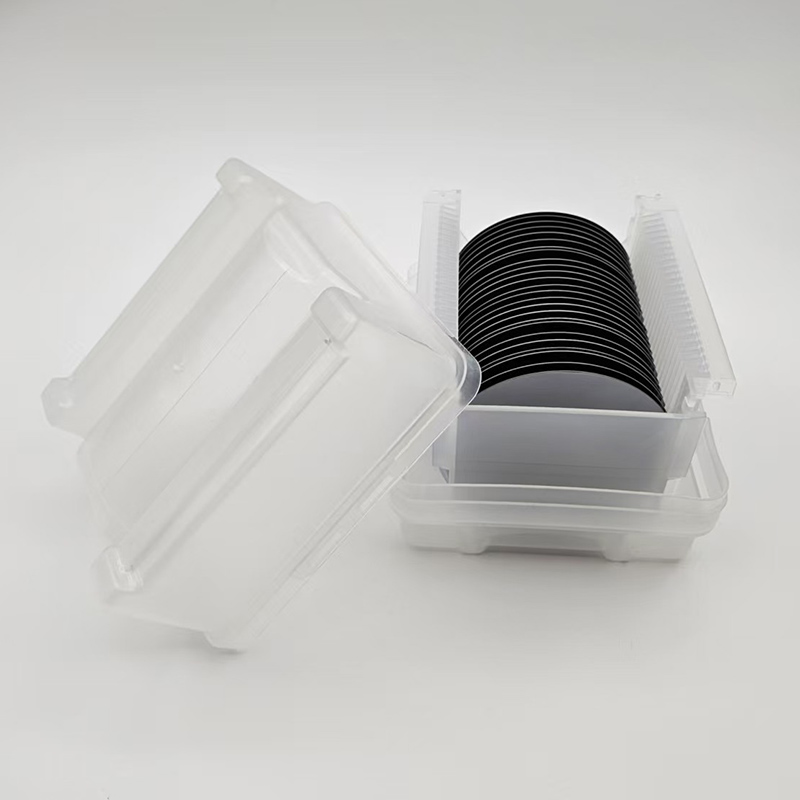
Packaging and Transportation
The packaging should be able to withstand the impact, vibration, stacking and extrusion that may be encountered during transportation, while also it has to easy to load, unload and handle.
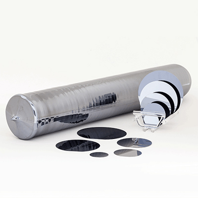
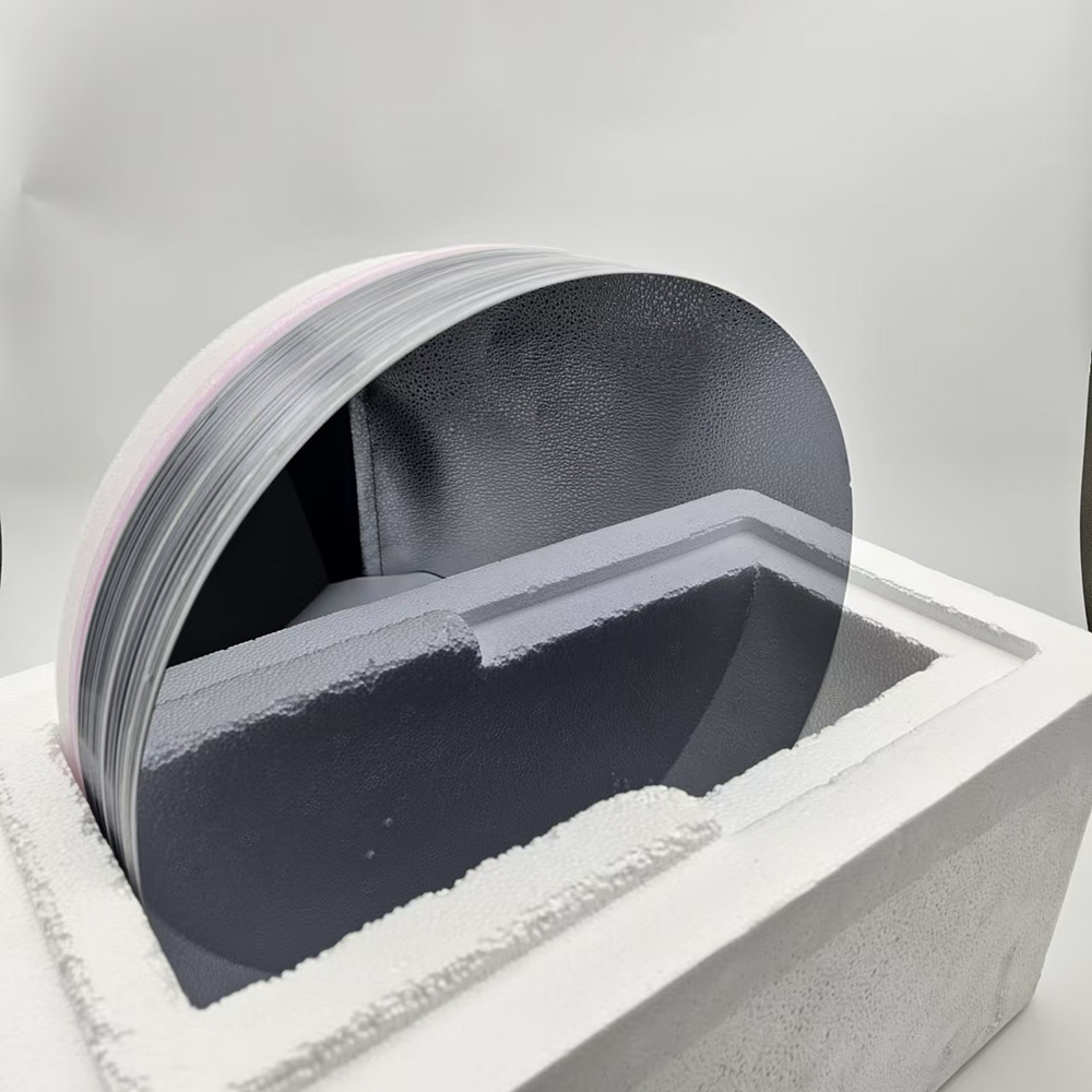
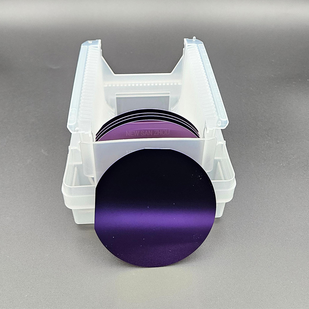
We use professional wafer box packaging. The wafer box is protected by a double layer bag, the inside is a PE bag that can be dust-proof, and the outside is a aluminum foil bag that can be isolated from the air. The two-layer bags are vacuum-packed.
We will choose carton models according to different sizes of products. And between the product and the carton filled with shock-proof EPE foam, play a comprehensive protection.
Finally choose air transport to reach the customer's hands. This allows customers in any country and region to receive the product in the fastest time.
We comply with the Material Safety Data Sheet (MSDS) rules to ensure that the products transported are free of harmful substances and will not cause environmental pollution and explosion and other possible hazards.

Enterprise Strength
Factory Area: 3000 sq
Process:
1. Shaping→2. Edge Profile→3. Lapping→4. Polishing→5. Cleaning→6. Packing→7. Transportation
Capacity:
Glass Wafer --- 30K pcs
Silicon Wafer --- 20K pcs
(Equal to 6in)

Quality Assurance
Quality inspection method: Product inspection in accordance with SEMI standard or according to customer's requirements, together with product COA.
Warranty period: In accordance with the contract requirements.
Quality system management:
●Organize production according to ISO9001 and other quality system standards.
Quality management system and measures:
●Establish a strict quality assurance system, the heads of all departments and quality engineers to ensure the coordinated operation of the quality system.
●Strengthen the quality inspection system, strengthen the process quality control
●Strict material quality control, ensure that the input materials meet the design requirements and technical specifications.
●Implement a timely filing system for technical data to ensure that all processing technical data is complete/accurate.
Quality control in the production stage:
●Production preparation stage: carefully organize relevant personnel to learn product drawings and technical rules, and improve the technical level of employees.
●Quality control of the production process: the implementation of a strict handover system, the previous step of the process to the next step of the transfer, should be detailed processing. At the same time, strengthen the quality inspection system to ensure the quality of each step of the process.
●Quality acceptance: All processes must be quality acceptance before proceeding to the next process.

Pre-sales and After-sales
Pre-sales Service
Professional technical support and commercial team to help you determine product specifications according to product use, and issue specifications.
On-purchase Service
Produce products according to the confirmed specifications and our process.
After Sale Service
We will respond to any product problems encountered by customers or process problems encountered by customers within 24 hours. We can choose from various forms of service, such as email, video conference and so on.
Plutosemi Co., Ltd. was established in 2019, headquartered in Nanhai, Foshan, focusing on the research and development, production, and sales of high-performance semiconductor materials.
Advanced production capacity: We have three major production bases in China, with a monthly production capacity of 100000 equivalent 6-inch silicon wafers and 30000 equivalent 8-inch glass wafers, ensuring stable and efficient product supply for our customers.
High quality products: We provide efficient and stable product supply innovative solutions in the fields of glass wafers, silicon polishing wafers, epitaxial wafers (EPI), silicon on insulator wafers (SOI), and more. Our silicon wafers have the characteristics of ultra-thin, ultraflat, and high-precision, which can meet the needs of various high-end applications. Our glass and quartz substrates are also renowned for their high smoothness and precise aperture design.