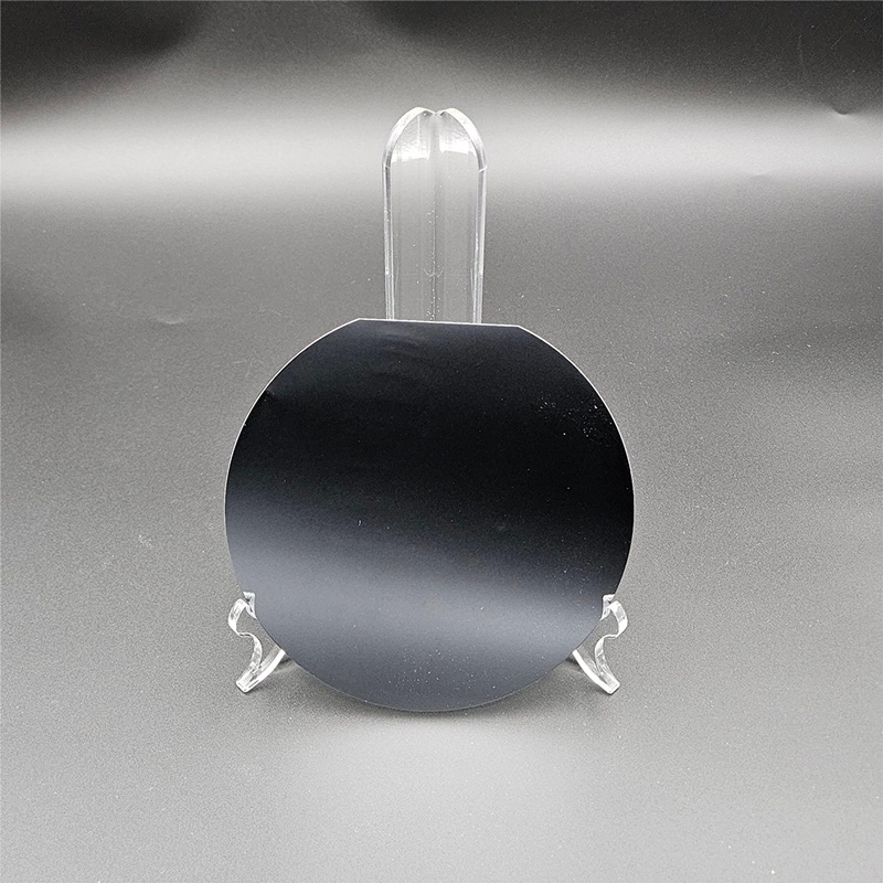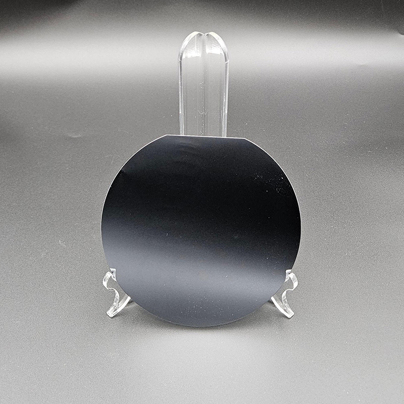
Thermal Oxide Silicon Wafer
Silicon Wafer

-
+86-17701852595 WhatsApp
-
sales@plutosemitech.com Email
Thermal Oxide Silicon Wafer is a type of silicon wafer in which a layer of silicon dioxide (SiO₂) is grown on the surface of a silicon wafer through a high-temperature oxidation process. This type of oxide layer is formed on the bare surface of silicon wafers under high temperature conditions with oxidants. The thermal oxidation layer is usually grown in a horizontal tube furnace, with a growth temperature range of 900 ℃~1200 ℃, and there are two growth methods: "wet oxidation" and "dry oxidation". The thermal oxide layer is a type of oxide layer that is "grown" and has higher uniformity and dielectric strength compared to the oxide layer deposited by CVD.

Thermal Oxide Silicon Wafer Specifications
| Product Name | Thermal oxide Silicon wafer (SiO₂/Si) Oxide layer on Silicon wafer Thermal oxidation of Silicon wafer |
| Oxide-layer(SiO₂ layer) | 25nm, 50nm, 100nm, 300nm, 500nm, 1μm or others |
| Oxidation surface | Single-sided oxidation, Double-sided oxidation |
| Oxidation process | Dry oxidation, Wet oxidation, |
| Conductivity type/Dopant | N-type/Phos-doped or N-type/As-doped or P-type/Boron-doped or Un-doped |
| Orientation | < 100 > or < 111 > |
| Diameter of Silicon wafer | 2"(50.8mm), 3"(76.2mm), 4"(100mm), 6"(150mm), 8"(200mm), 12"(250mm) |
| Thickness of Silicon wafer | 280μm, 380μm, 525μm, 675μm, 725μm |
| Resistivity (Ohm-cm) | 0.001~0.005, 0.01~0.09, 0.1~0.9, 1~10, 20~30, > 100, > 1000, >10000 |
| Polishing | Single side polished or Double side polished |
| Surface Roughness | Ra < 5A (0.5nm) or Ra < 10A (1.0nm) |
| OEM/ODM | Accept |
| Compay Nature | China Manufacturers Suppliers Factory |
Thermal Oxide Silicon Wafer Features
1. Excellent electrical performance
Thermal Oxide Silicon Wafer, as an insulator or amorphous semiconductor material, exhibits excellent insulation performance and thermal stability. Its specific capacitance at room temperature is relatively low, about 3.9, and decreases with increasing temperature. Its high insulation performance means that even in complex circuit environments, it can effectively prevent signal interference and current leakage, thereby ensuring the overall performance of the device.
2. Good controllability
The key parameters of silicon thermal oxidation process, including temperature, atmosphere, and time, can be precisely controlled. Temperature, as the main factor affecting the oxidation rate and quality of the oxide layer, can significantly promote the progress of the oxidation reaction. In terms of atmosphere, oxygen is usually used as an oxidant, and by adjusting the flow rate of oxygen, the oxidation rate can be precisely controlled. The reaction time directly determines the thickness of the oxide layer. In actual production, by strictly controlling these process parameters, precise control of the thickness, uniformity, and quality of the oxide layer can be achieved, thereby meeting the design requirements of various complex devices.
3. High quality oxide film
The oxide film formed by dry oxygen oxidation has a dense structure, good uniformity, and repeatability. Its surface presents a non-polar siloxane structure, which adheres well to photoresist and is not easy to float. Due to its relatively slow oxidation rate, dry oxygen oxidation is usually suitable for forming thin high-quality oxide layers.
4. Efficient wet oxygen oxidation process
The wet oxygen oxidation process significantly improves the oxidation rate by introducing water vapor as an oxidant. Due to the decomposition of water vapor into hydrogen oxide at high temperatures, its diffusion rate in silicon oxide is much faster than that of oxygen, so the wet oxygen oxidation rate is about an order of magnitude higher than the dry oxygen oxidation rate. Although impurities or defects may be introduced during the wet oxygen oxidation process, it is still possible to obtain an oxide layer that meets the performance requirements of the device by strictly controlling the process conditions.
5. Excellent uniformity and density
Compared with other methods such as chemical vapor deposition (CVD), the oxide layer formed by thermal oxidation has better uniformity and density. The oxide layer formed by dry oxidation has higher density and more uniform structure, which can effectively reduce the occurrence of defects and pinholes. This excellent uniformity and density ensure the consistency of device performance, improving the reliability and stability of the product.
6. High dielectric strength
Thermal silicon oxide has high dielectric strength and can withstand large electric field strengths without breakdown. This characteristic makes thermally oxidized silicon an ideal material for manufacturing high-voltage devices. Under high voltage conditions, thermally oxidized silicon can maintain stable electrical performance, ensuring the safe operation of the device. Its high dielectric strength not only improves the voltage resistance of the device, but also provides the possibility for the compactness and high performance of the device.
7. Good high-temperature stability
Thermal silicon oxide can maintain stable physical and chemical properties in high temperature environments. The high-temperature stability of thermally oxidized silicon ensures that it will not undergo performance degradation or structural changes during these process steps, thereby ensuring the overall quality and reliability of the device. This excellent high-temperature stability makes thermal silicon oxide widely used in various high-temperature process scenarios, providing strong support for the manufacturing of semiconductor devices.
Thermal Oxide Silicon Wafer Process Flow
The production process of Thermal Oxide Silicon Wafer mainly includes the following key steps:
1. Silicon wafer cleaning: Firstly, strict cleaning treatment is carried out on the original silicon wafer to remove impurities and pollutants on the surface, ensuring the quality of the oxidation process.
2. Preparation of oxidation furnace: Place the cleaned silicon wafer into a quartz tube oxidation furnace. Quartz tubes have high melting points and chemical stability, and can withstand high-temperature oxidation environments.
3. Temperature control: Precise temperature control of the oxidation furnace is achieved through multiple heating zones, stabilizing the temperature inside the furnace between 1000 ° C and 1200 ° C and providing sufficient energy for the oxidation reaction.
4. Introduction of oxidation atmosphere: According to the process requirements, introduce pure oxygen or an oxidation atmosphere containing water vapor into the oxidation furnace. Dry oxygen oxidation uses pure oxygen as an oxidant to form high-quality oxide films; Wet oxygen oxidation enhances the oxidation reaction rate through water vapor.
5. Oxidation process monitoring: During the oxidation process, the growth rate and uniformity of the oxide layer are monitored in real time, and the quality of the oxide layer is ensured by adjusting process parameters.
6. Cooling and removal from the furnace: After oxidation is complete, slowly reduce the temperature inside the furnace to room temperature to avoid cracking or deformation of the silicon wafer due to rapid temperature changes. Finally, remove the Thermal Oxide Silicon Wafer for subsequent processing and testing.
Thermal Oxide Silicon Wafer Application
1. MOSFET gate oxide
Thermal Oxide Silicon Wafer plays a crucial role as the gate oxide in MOSFETs (metal oxide semiconductor field-effect transistors). It has good insulation and low surface state density, which can effectively control the modulation effect of gate voltage on channel current and achieve the switching function of the device. The gate oxide layer is usually prepared by thermal oxidation method, forming a silicon oxide layer with extremely low leakage current and high breakdown electric field strength, ensuring the stability and reliability of the device.
2. IC process dielectric layer
In the integrated circuit (IC) process, Thermal Oxide Silicon Wafer is widely used as a dielectric layer for electrical isolation, surface protection, and masking. Its excellent electrical insulation, thermal stability, and chemical stability make it one of the most commonly used dielectric layer materials in the semiconductor industry.
3. Insulation and mask materials
Thermal silicon oxide is not only used as an insulating layer in semiconductor processes, but also as a mask material, with high selectivity and chemical inertness. It can effectively prevent the erosion of chemical reagents or gases, accurately define the diffusion boundary of doping elements, and ensure precise control of the doping area. In key steps such as etching, diffusion, and ion implantation, Thermal Oxide Silicon Wafer acts as a mask layer to protect areas that do not require processing, improving the accuracy and efficiency of the process.
4. Solar silicon chips
In the field of solar cells, Thermal Oxide Silicon Wafer plays an important role as a surface passivation layer. It can effectively reduce the surface recombination rate of silicon wafers and improve the photoelectric conversion efficiency of batteries. The fixed positive charges formed during the thermal oxidation process will generate field effect passivation, further reducing the density of surface defect states and improving the performance of the battery.
5. Epitaxial silicon wafer
In the preparation process of epitaxial silicon wafers, thermally oxidized silicon serves as an intermediate layer, providing a flat and clean surface for epitaxial growth. It can effectively block impurity diffusion, protect active devices and silicon from the influence of subsequent processes. The quality of the thermally oxidized silicon layer is crucial for the growth quality of the epitaxial layer and the performance of the device.
Packaging and Transportation
The packaging should be able to withstand the impact, vibration, stacking and extrusion that may be encountered during transportation, while also it has to easy to load, unload and handle.
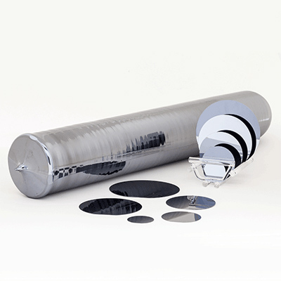
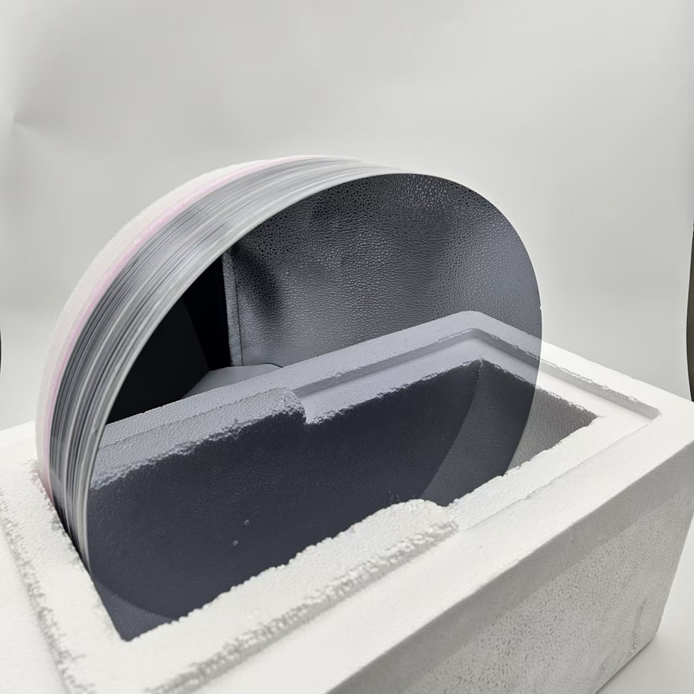
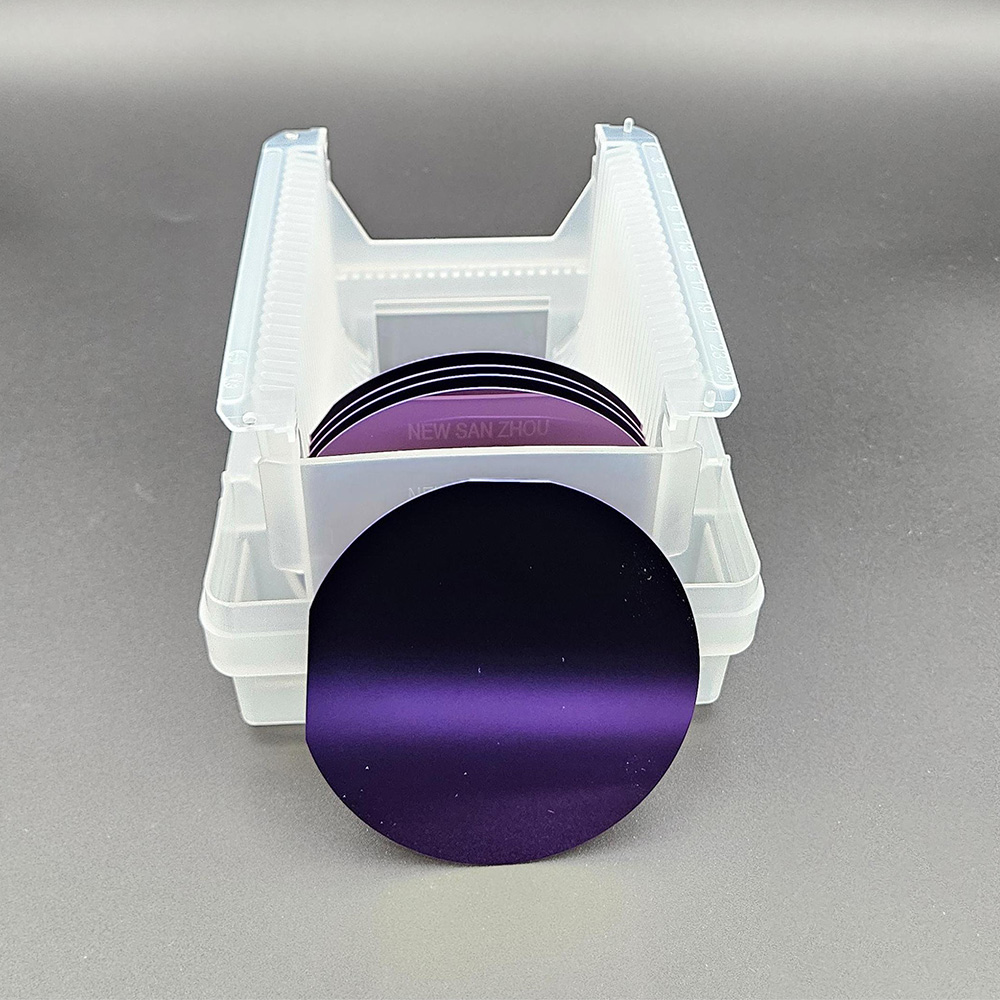
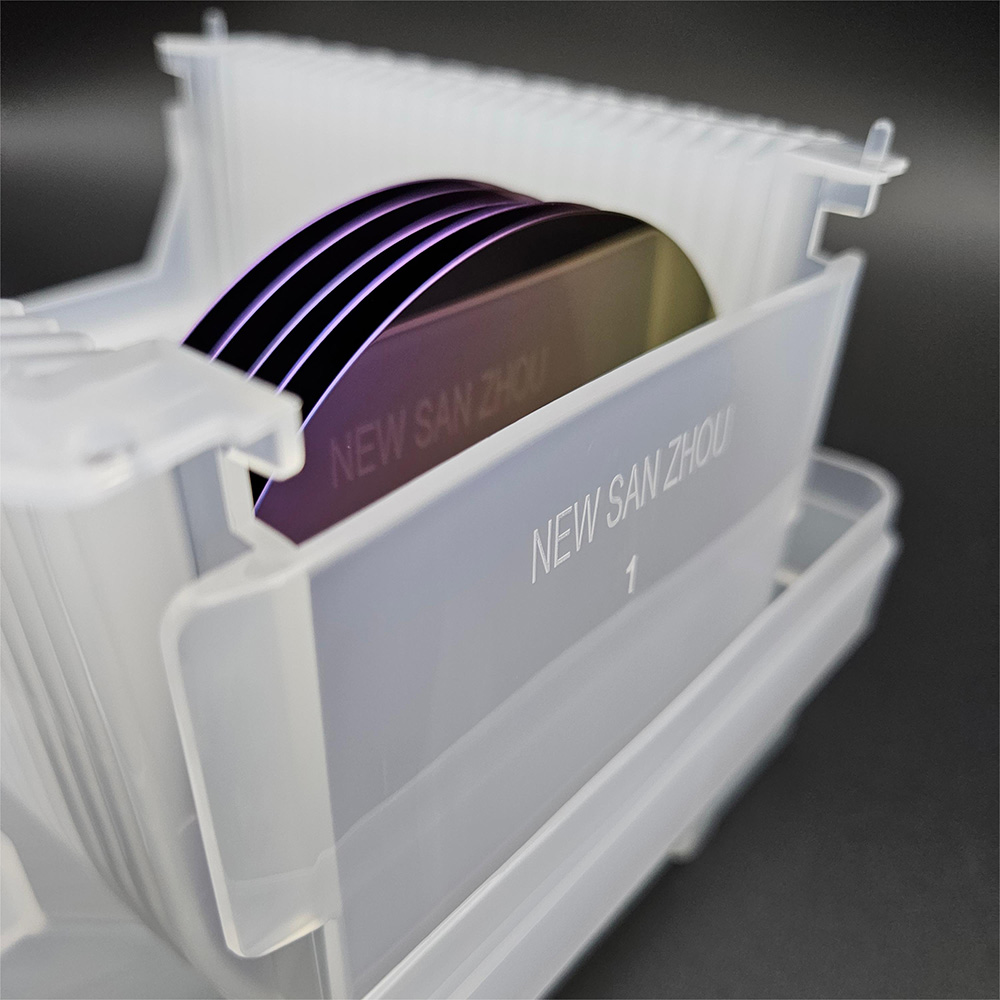
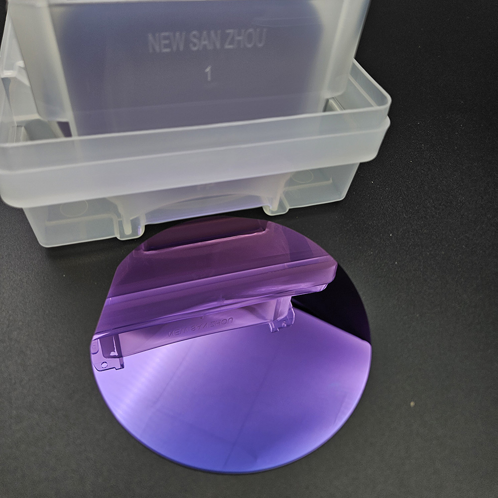
We use professional wafer box packaging. The wafer box is protected by a double layer bag, the inside is a PE bag that can be dust-proof, and the outside is a aluminum foil bag that can be isolated from the air. The two-layer bags are vacuum-packed.
We will choose carton models according to different sizes of products. And between the product and the carton filled with shock-proof EPE foam, play a comprehensive protection.
Finally choose air transport to reach the customer's hands. This allows customers in any country and region to receive the product in the fastest time.
We comply with the Material Safety Data Sheet (MSDS) rules to ensure that the products transported are free of harmful substances and will not cause environmental pollution and explosion and other possible hazards.

Enterprise Strength
Factory Area: 3000 sq
Process:
1. Shaping→2. Edge Profile→3. Lapping→4. Polishing→5. Cleaning→6. Packing→7. Transportation
Capacity:
Glass Wafer --- 30K pcs
Silicon Wafer --- 20K pcs
(Equal to 6in)

Quality Assurance
Quality inspection method: Product inspection in accordance with SEMI standard or according to customer's requirements, together with product COA.
Warranty period: In accordance with the contract requirements.
Quality system management:
●Organize production according to ISO9001 and other quality system standards.
Quality management system and measures:
●Establish a strict quality assurance system, the heads of all departments and quality engineers to ensure the coordinated operation of the quality system.
●Strengthen the quality inspection system, strengthen the process quality control
●Strict material quality control, ensure that the input materials meet the design requirements and technical specifications.
●Implement a timely filing system for technical data to ensure that all processing technical data is complete/accurate.
Quality control in the production stage:
●Production preparation stage: carefully organize relevant personnel to learn product drawings and technical rules, and improve the technical level of employees.
●Quality control of the production process: the implementation of a strict handover system, the previous step of the process to the next step of the transfer, should be detailed processing. At the same time, strengthen the quality inspection system to ensure the quality of each step of the process.
●Quality acceptance: All processes must be quality acceptance before proceeding to the next process.

Pre-sales and After-sales
Pre-sales Service
Professional technical support and commercial team to help you determine product specifications according to product use, and issue specifications.
On-purchase Service
Produce products according to the confirmed specifications and our process.
After Sale Service
We will respond to any product problems encountered by customers or process problems encountered by customers within 24 hours. We can choose from various forms of service, such as email, video conference and so on.
Plutosemi Co., Ltd. was established in 2019, headquartered in Nanhai, Foshan, focusing on the research and development, production, and sales of high-performance semiconductor materials.
Advanced production capacity: We have three major production bases in China, with a monthly production capacity of 100000 equivalent 6-inch silicon wafers and 30000 equivalent 8-inch glass wafers, ensuring stable and efficient product supply for our customers.
High quality products: We provide efficient and stable product supply innovative solutions in the fields of glass wafers, silicon polishing wafers, epitaxial wafers (EPI), silicon on insulator wafers (SOI), and more. Our silicon wafers have the characteristics of ultra-thin, ultraflat, and high-precision, which can meet the needs of various high-end applications. Our glass and quartz substrates are also renowned for their high smoothness and precise aperture design.