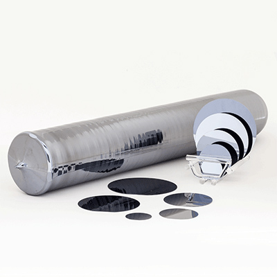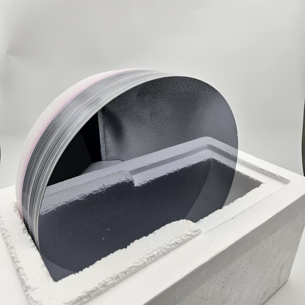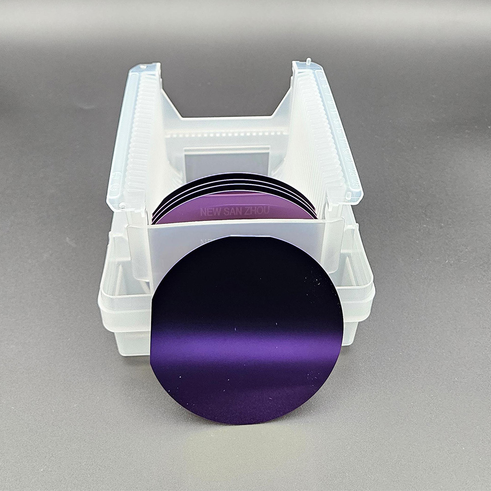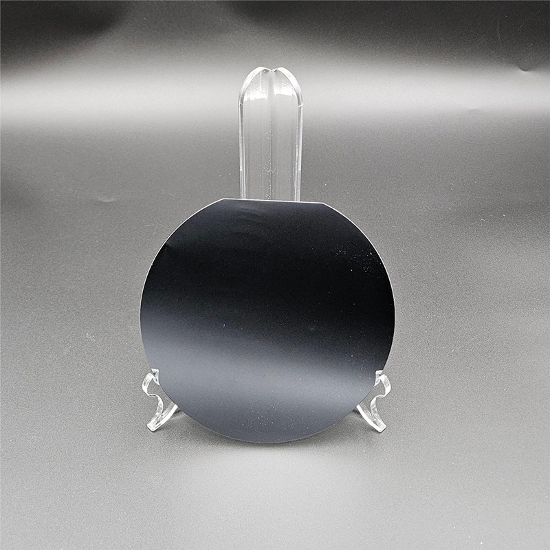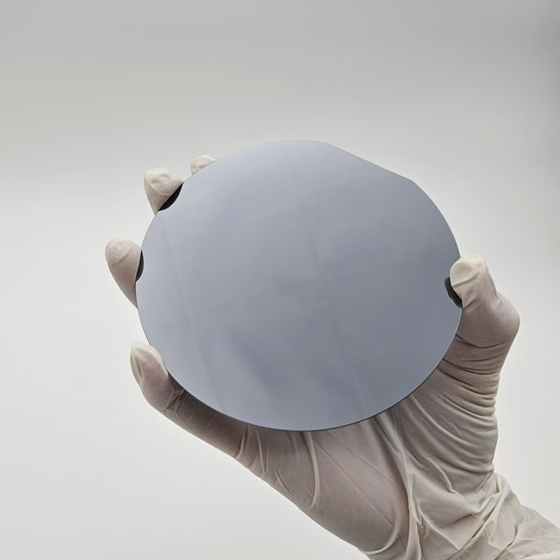
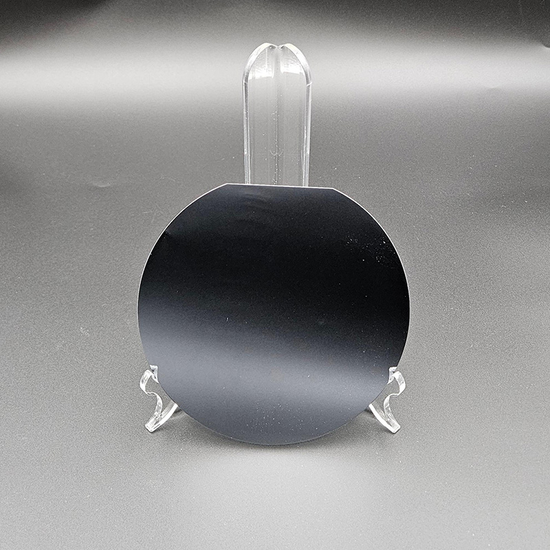
Ultra Flat Silicon Wafer
Silicon Wafer

-
+86-17701852595 WhatsApp
-
sales@plutosemitech.com Email
Ultra-Flatness Wafer can be used for the base substrate, which is applicable for bonding or photolithography processes, and will fit for good uniformity based on several deposition processes, which means proper substrate for accuracy demanded several devices. PLUTO will also apply better flatness quality as per the customer’s requirements and reach around 2μm. As a leading China ultra flat silicon wafer supplier, we provide wafers that ensure exceptional flatness and uniformity, even across multiple deposition processes.
Product Standard:
Diameter: 4, 6inch
TTV: ≤2μm (Actual: ≤1μm)
Type: P type/B, N type/Phos, N type/As, FZ
Orientation:< 100 >, < 111 >
Resistivity: ≤0.005~40Ωcm
Surface: DSP

Ultra Flat Silicon Wafer Specifications
| Item | 4 inch | 6 inch |
| Diameter(mm) | 100±0.2 | 150±0.2 |
| Thickness | 200-1500μm | 200-1500μm |
| TTV(μm) | ≤2μm (Actual: ≤1μm) | ≤2μm (Actual: ≤1μm) |
| Particles | ≤10ea@0.3μm | ≤10ea@0.3μm |
| Surface | DSP | DSP |
Ultra Flat Silicon Wafer FAQ
What is an ultra flat silicon wafer?
An ultra flat silicon wafer is a highly polished silicon substrate that maintains an exceptional level of flatness, often within micrometer range, to ensure uniformity in semiconductor manufacturing processes like photolithography and bonding.
Why is flatness important for silicon wafers?
Flatness is crucial for achieving high precision in device fabrication. Variations in flatness can lead to misalignment, defects, or inconsistencies in the performance of semiconductor devices, impacting overall yield and quality.
What applications are ultra-flat silicon wafers used in?
Ultra-flat silicon wafers are primarily used in semiconductor fabrication, including photolithography, bonding, MEMS (Micro-Electro-Mechanical Systems), and optoelectronic devices, where high precision and uniformity are required.
How flat can your ultra-flat silicon wafers get?
Our ultra-flat silicon wafers can reach a flatness tolerance as low as 2μm, depending on customer requirements, ensuring superior performance and reliability in precision applications.
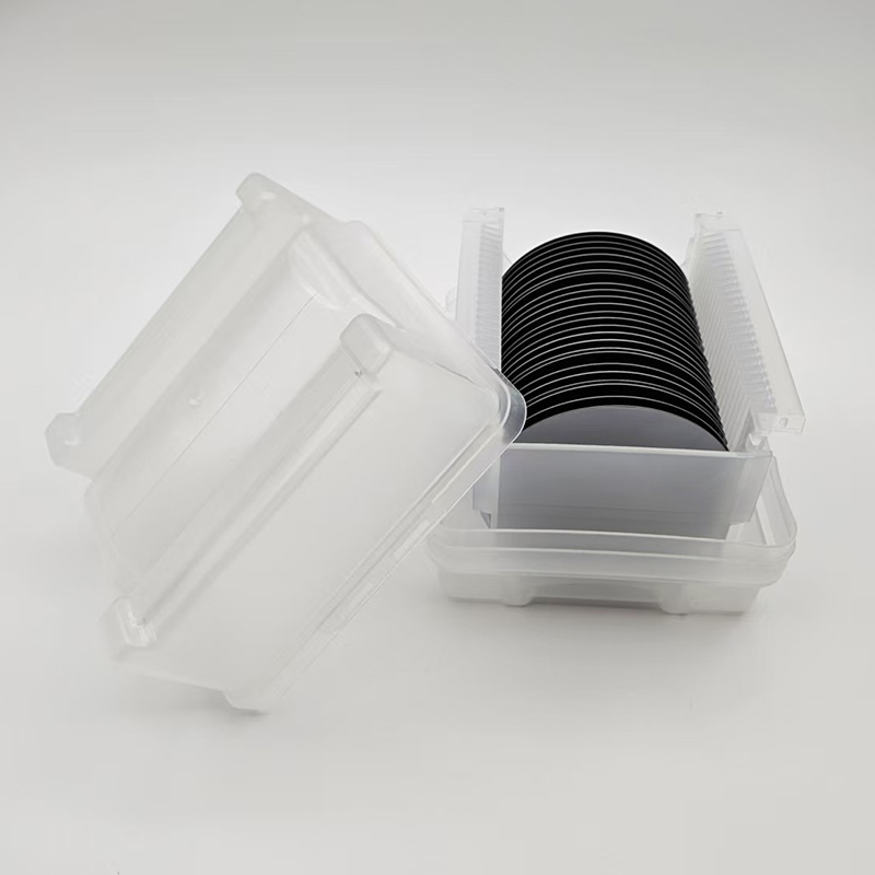
Packaging and Transportation
The packaging should be able to withstand the impact, vibration, stacking and extrusion that may be encountered during transportation, while also it has to easy to load, unload and handle.
We use professional wafer box packaging. The wafer box is protected by a double layer bag, the inside is a PE bag that can be dust-proof, and the outside is a aluminum foil bag that can be isolated from the air. The two-layer bags are vacuum-packed.
We will choose carton models according to different sizes of products. And between the product and the carton filled with shock-proof EPE foam, play a comprehensive protection.
Finally choose air transport to reach the customer's hands. This allows customers in any country and region to receive the product in the fastest time.
We comply with the Material Safety Data Sheet (MSDS) rules to ensure that the products transported are free of harmful substances and will not cause environmental pollution and explosion and other possible hazards.

Enterprise Strength
Factory Area: 3000 sq
Process:
1. Shaping→2. Edge Profile→3. Lapping→4. Polishing→5. Cleaning→6. Packing→7. Transportation
Capacity:
Glass Wafer --- 30K pcs
Silicon Wafer --- 20K pcs
(Equal to 6in)

Quality Assurance
Quality inspection method: Product inspection in accordance with SEMI standard or according to customer's requirements, together with product COA.
Warranty period: In accordance with the contract requirements.
Quality system management:
●Organize production according to ISO9001 and other quality system standards.
Quality management system and measures:
●Establish a strict quality assurance system, the heads of all departments and quality engineers to ensure the coordinated operation of the quality system.
●Strengthen the quality inspection system, strengthen the process quality control
●Strict material quality control, ensure that the input materials meet the design requirements and technical specifications.
●Implement a timely filing system for technical data to ensure that all processing technical data is complete/accurate.
Quality control in the production stage:
●Production preparation stage: carefully organize relevant personnel to learn product drawings and technical rules, and improve the technical level of employees.
●Quality control of the production process: the implementation of a strict handover system, the previous step of the process to the next step of the transfer, should be detailed processing. At the same time, strengthen the quality inspection system to ensure the quality of each step of the process.
●Quality acceptance: All processes must be quality acceptance before proceeding to the next process.

Pre-sales and After-sales
Pre-sales Service
Professional technical support and commercial team to help you determine product specifications according to product use, and issue specifications.
On-purchase Service
Produce products according to the confirmed specifications and our process.
After Sale Service
We will respond to any product problems encountered by customers or process problems encountered by customers within 24 hours. We can choose from various forms of service, such as email, video conference and so on.
Plutosemi Co., Ltd. was established in 2019, headquartered in Nanhai, Foshan, focusing on the research and development, production, and sales of high-performance semiconductor materials.
Advanced production capacity: We have three major production bases in China, with a monthly production capacity of 100000 equivalent 6-inch silicon wafers and 30000 equivalent 8-inch glass wafers, ensuring stable and efficient product supply for our customers.
High quality products: We provide efficient and stable product supply innovative solutions in the fields of glass wafers, silicon polishing wafers, epitaxial wafers (EPI), silicon on insulator wafers (SOI), and more. Our silicon wafers have the characteristics of ultra-thin, ultraflat, and high-precision, which can meet the needs of various high-end applications. Our glass and quartz substrates are also renowned for their high smoothness and precise aperture design.