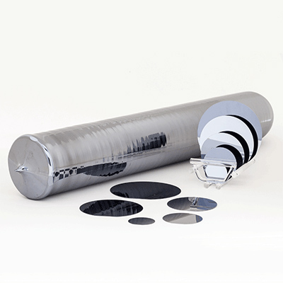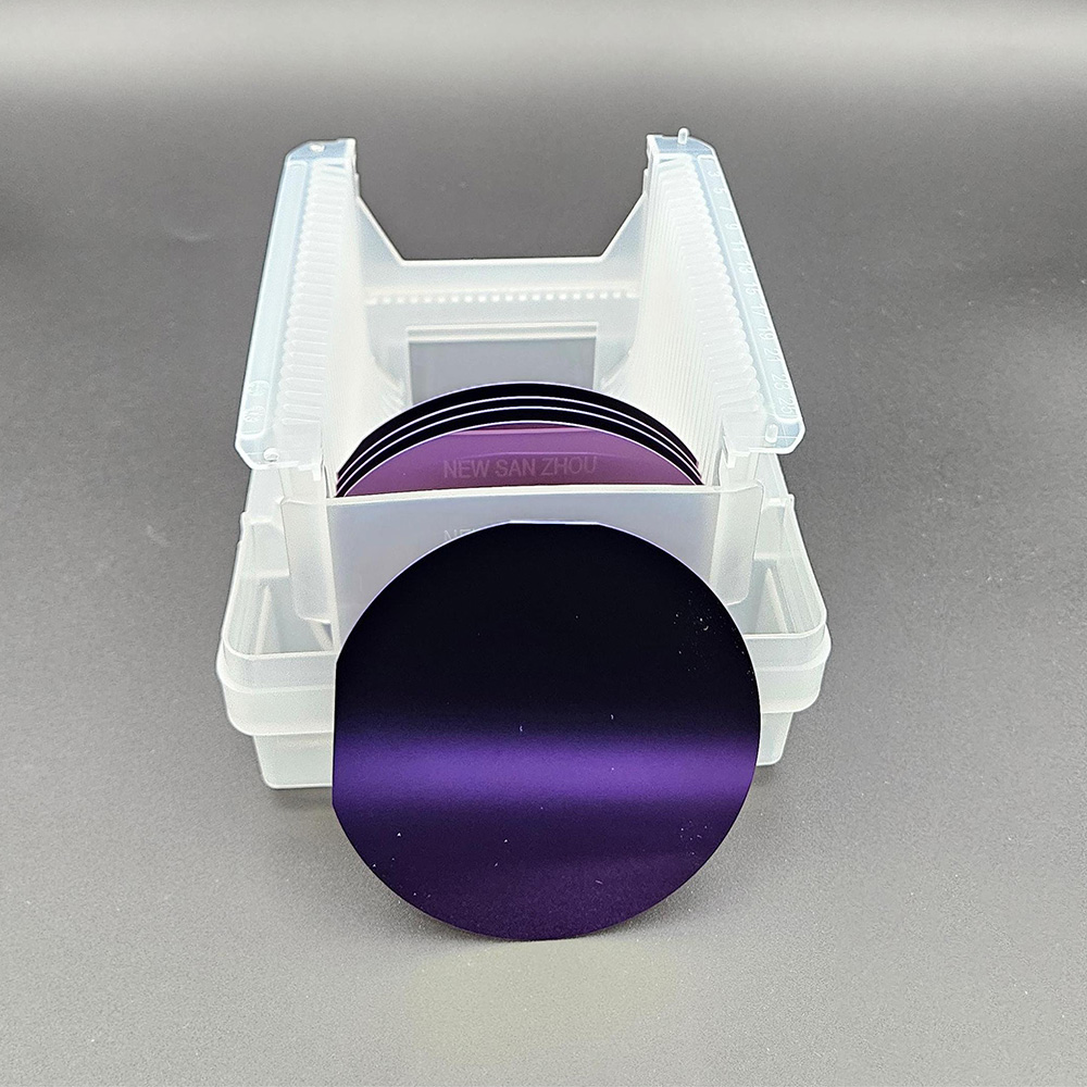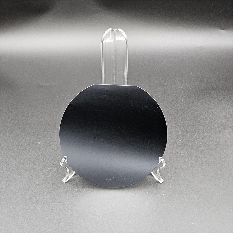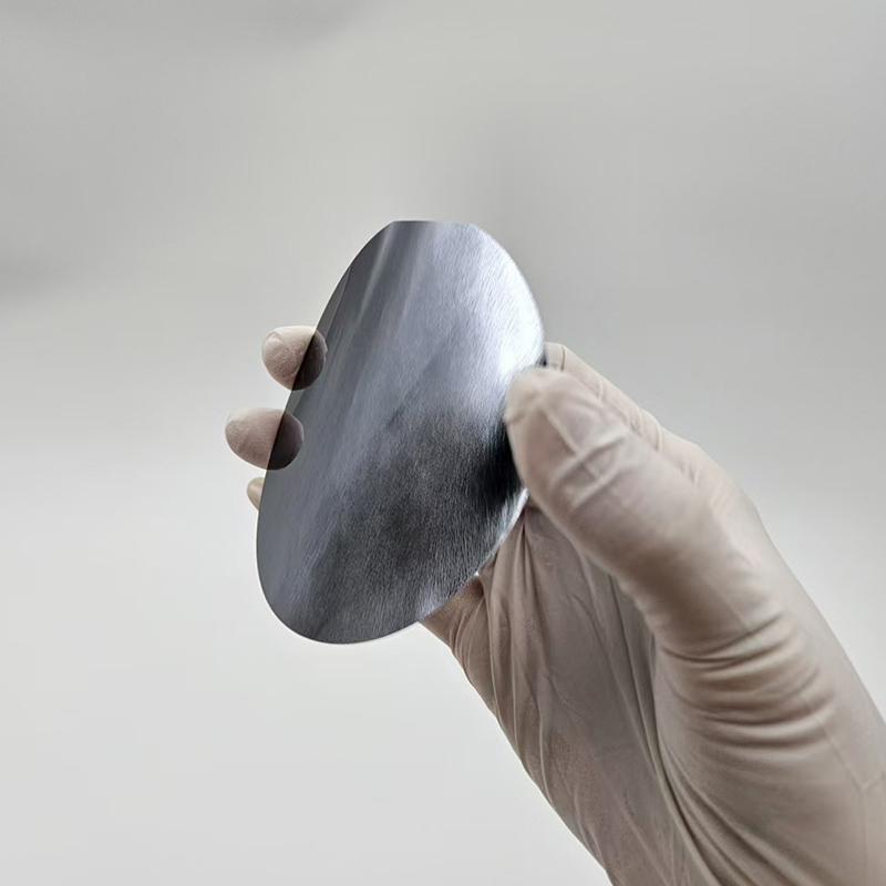
Ultra Thin Silicon Wafer
Silicon Wafer

-
+86-17701852595 WhatsApp
-
sales@plutosemitech.com Email
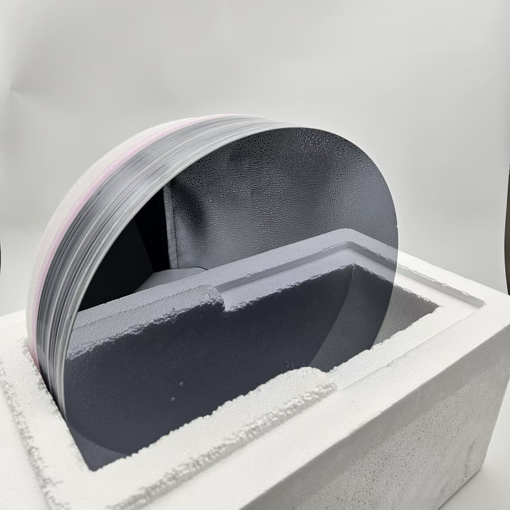
Ultra Thin Silicon Wafer refers to silicon wafers with a thickness ranging from tens of micrometers to hundreds of micrometers. This type of wafer plays a crucial role in modern semiconductor manufacturing processes, especially in MEMS (Micro Electro Mechanical Systems) processes. In MEMS technology, customers often use it with a thickness between 50 μ m and 100 μ m. These silicon wafers can meet the requirements of MEMS devices for high precision, high integration, and complex structures. Meanwhile, the processing of ultra-thin silicon wafers is also a challenging technology that requires advanced equipment and processes to achieve.

Ultra Thin Silicon Wafer Specifications
| Diameters | 4, 5, 6, 8,12 inches |
| Thickness | 100-150μm |
| Particle | ≧ 0.3μm,≦ 50ea/wf |
| Metals | ≦ 5.0E10atoms/cm-2(Ka, Ca, Ti, Cr, Mn, Fe, Co, Ni, Cu, Zn, Al, Na) |
Ultra Thin Silicon Wafer Features
1. Consistency of thickness:
The Ultra Thin Silicon Wafer can be controlled between tens of micrometers and hundreds of micrometers, and can even reach thinner levels. Its thickness distribution is very uniform, thanks to advanced manufacturing and polishing technology, ensuring the consistency of the thickness of the silicon wafer on the entire surface.
2. High flexibility and toughness:
Despite its extremely thin thickness, ultra-thin silicon wafers still maintain good flexibility and elasticity, and can withstand a certain degree of bending and deformation without breaking. This characteristic makes ultra-thin silicon wafers more flexible in processing and handling, making it easier to achieve complex shape and structural designs.
3. Nano level surface smoothness:
The manufacturing process of ultra thin silicon wafer involves precise machining and polishing techniques to ensure that their surfaces achieve nanometer level flatness. This high precision is crucial for subsequent device manufacturing and precise formation of circuit patterns.
4. Excellent semiconductor performance:
Silicon, as a typical semiconductor material, has excellent conductivity and doping properties. Ultra thin silicon wafers maintain these excellent properties of silicon, allowing for P-type or N-type doping as needed, as well as adjusting resistivity.
5. Good thermal and chemical stability:
Ultra thin silicon wafers can withstand high-temperature processing steps such as annealing and thermal oxidation without significant deformation or performance degradation. At the same time, it exhibits good resistance to many chemicals and can maintain its integrity during chemical etching and cleaning processes.
6. Optical characteristics:
When the thickness is reduced to a certain extent, ultra-thin silicon wafers can exhibit a certain degree of optical transparency, allowing light to penetrate. This characteristic provides the possibility for the application of ultra-thin silicon wafers in the optical field, although their main applications are still concentrated in the fields of electronics and microelectromechanical systems.
7. Customizability and Diversity:
The thickness, size, shape, and doping type of ultra-thin silicon wafers can be customized according to customer needs. This flexibility enables ultra-thin silicon wafers to meet specific needs in different fields and applications.
Ultra Thin Silicon Wafer Process Flow
1. Paste a Protective Film
● Purpose: In the processing of ultra thin silicon wafer, in order to protect their surface from mechanical damage and contamination, a protective film needs to be attached to the surface of the silicon wafer.
● Operation: Use specialized film sticking equipment to evenly stick the protective film onto the surface of the silicon wafer. Protective films usually have good adhesion and wear resistance, which can effectively protect the surface of silicon wafers.
2. Single Polishing
● Purpose: To remove micro defects, stress damage layers, and impurities such as metal ions from the surface of silicon wafers through polishing technology, and improve the flatness and roughness of the silicon wafer surface.
● Operation:
Fix the silicon wafer coated with protective film onto the polishing machine.
Using specialized polishing solution and polishing cloth, polish the surface of silicon wafers under precisely controlled temperature, pressure, and rotation speed.
During the polishing process, the chemical components in the polishing solution react chemically with the surface of the silicon wafer, while the mechanical friction of the polishing cloth removes surface micro defects and impurities.
3. Processing Surface Non contact Film Stripping
● Purpose: After polishing, it is necessary to peel off the protective film attached to the surface of the silicon wafer while avoiding secondary damage to the silicon wafer surface.
● Operation:
Using non-contact thin film peeling equipment, the protective film is peeled off from the surface of the silicon wafer through physical or chemical methods.
Non contact exfoliation can reduce mechanical stress on the surface of silicon wafers, avoiding scratches or damage.
4. Cleaning
● Purpose: To remove residual polishing solution, impurities, and possible microcracks and damage layers on the surface of silicon wafers, ensuring the purity and quality of the silicon wafer surface.
● Operation:
Various cleaning methods are used, such as ultrasonic cleaning, chemical cleaning, etc., to thoroughly clean the surface of silicon wafers.
Ultrasonic cleaning uses ultrasonic vibration to remove surface impurities and particles; Chemical cleaning uses specific chemical solutions to undergo chemical reactions with the surface of silicon wafers, removing residues and damaged layers.
During the cleaning process, it is necessary to strictly control the composition, temperature, and cleaning time of the cleaning solution to avoid corrosion or damage to the surface of the silicon wafer.
Ultra Thin Silicon Wafer Application
1. Microelectronics packaging field
LED packaging: Ultra thin silicon wafer can be used as LED packaging substrates, providing excellent thermal conductivity and mechanical strength, while reducing packaging volume and improving packaging efficiency.
CMOS image sensor and MEMS sensor packaging: The high-precision processing characteristics of ultra-thin silicon wafers enable them to meet the high requirements of packaging materials for these microelectronic devices, achieving finer packaging structures.
2. Chip manufacturing field
Integrated circuit manufacturing: Ultra thin silicon wafers are important materials for manufacturing high-performance integrated circuits. Through precise grinding and polishing, high-precision processing requirements can be achieved, improving the integration and performance of integrated circuits.
Production of solar cells and LED chips: It is also widely used in the production of solar cells and LED chips, which can improve solar energy conversion efficiency and LED luminous efficiency.
3. In the field of optoelectronics
Photonic devices: Ultra thin silicon wafers have become an important component of photonic devices due to their excellent optical properties and preparability, providing a solid foundation for the development of fields such as lasers and optical communications.
4. Biomedical field
Biochips: Ultra thin silicon wafers can be used to manufacture biochips, providing new tools for disease diagnosis and genetic research. Through surface engineering and functionalization, silicon wafers can become sensitive materials for biosensors, achieving efficient detection of biomolecules.
Medical implants: Ultra thin silicon wafers can also be used to manufacture implantable medical devices such as flexible electronic skin, neural interfaces, etc. Due to their flexibility and biocompatibility, they can better integrate with human tissues.
5. Flexible electronics field
Flexible Display: It can serve as substrate materials for flexible displays, enabling thinner and more flexible display devices, providing new display solutions for wearable devices, smartphones, and more.
Flexible sensors: It can be used to manufacture various flexible sensors, such as pressure sensors, temperature sensors, etc. These sensors can be integrated into clothing, skin, or other flexible surfaces to achieve real-time monitoring of human health, exercise status, etc.
6. Adaptive Optical Imaging Technology
Deformable mirror production: Ultra thin silicon wafers can be used to produce deformable mirrors in adaptive optics systems, compensating for imaging distortions caused by atmospheric turbulence and improving optical imaging quality by changing the surface shape.
Plutosemi Co., Ltd. was established in 2019, headquartered in Nanhai, Foshan, focusing on the research and development, production, and sales of high-performance semiconductor materials.
Advanced production capacity: We have three major production bases in China, with a monthly production capacity of 100000 equivalent 6-inch silicon wafers and 30000 equivalent 8-inch glass wafers, ensuring stable and efficient product supply for our customers.
High quality products: We provide efficient and stable product supply innovative solutions in the fields of glass wafers, silicon polishing wafers, epitaxial wafers (EPI), silicon on insulator wafers (SOI), and more. Our silicon wafers have the characteristics of ultra-thin, ultraflat, and high-precision, which can meet the needs of various high-end applications. Our glass and quartz substrates are also renowned for their high smoothness and precise aperture design.