


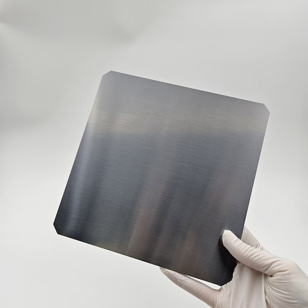
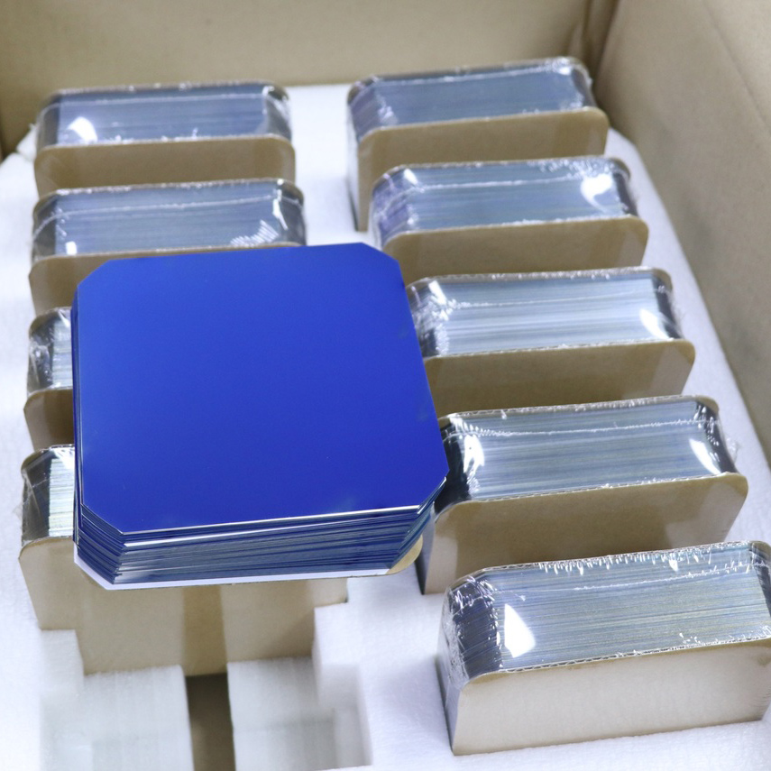
Monocrystalline Solar Wafer
Solar Wafers

-
+86-17701852595 WhatsApp
-
sales@plutosemitech.com Email
Monocrystalline Solar Wafer is a core material used in the manufacturing of solar cells and belongs to a type of monocrystalline silicon wafer. It is made of high-purity single crystal silicon and has a highly ordered crystal structure, which makes its internal atomic arrangement extremely regular and uniform. Monocrystalline silicon is a thin sheet formed by cutting a single crystal grown from a molten state through a specific method, hence it is called a "single crystal". Compared with other types of silicon wafers, Monocrystalline Solar Wafer is known for its high purity and fewer crystal defects, and occupies an important position in the energy field.

Monocrystalline Solar Wafer Specifications
Material Properties:
| Crystal Growth Method | CZ |
| ConductivityType/Dopant | P/Boron, P/gallium |
| Oxygen Concentration | ≤ 8.0×10¹⁷ atoms/cm³ |
| Carbon Concentration | ≤ 5.0×10¹⁶ atoms/cm³ |
| Crystal orientation | < 100 >±3° |
| Dislocation Density | ≤ 500/cm2 |
Electrical Properties:
| Resistivity | [0.5~1.5]Ω.cm |
| Brick Lifetime | LT ≥ 70μs(BCT-400) |
Geometry & Surface:
| Wafer Dimention | 182*182mm | |
| Thickness | (140/145/150/155/160) ±10μm | |
| TTV | ≤ 25μm | |
| Saw mark | ≤ 13μm | |
| Warpage | ≤ 40μm | |
| Width | 182 ±0.25mm | |
| Right(Rectangular) Angle | 90°±0.15° | |
| Chamfer Size | Chord length | 10.62±0.7mm |
| Chamfer Cathetus | 7.51±0.45mm | |
| Diagonal | 247±0.25mm | |
| Microcrack | Not allowed | |
| Edge Chip | Depth ≤ 0.3 mm ,Length ≤ 0.5 mm, Max 1 pieces/wafer; V-shape crack unacceptable | |
| Surface quality | No surface stains, water marks, breakage or hole allowed | |
Monocrystalline Solar Wafer Features
1. Crystal growth method: Czochralski (CZ) method
Monocrystalline Solar Wafer uses the Czochralski method for crystal growth, which is currently one of the most mature and widely used technologies. This method involves immersing a small single crystal seed into molten silicon and slowly rotating it to form a large-sized single crystal rod. This method can precisely control the growth rate and direction of the crystal, ensuring that the final silicon wafer has an almost perfect crystal structure. In addition, the CZ method can effectively reduce impurity content, improve the overall quality of silicon wafers, and make them more suitable for high-performance photovoltaic applications.
2. Conductive type and doping elements
This Monocrystalline Solar Wafer offers two conductivity types to choose from: P-type/boron doped (P/Boron) and P-type/gallium doped (P/Gallium). These two doping methods each have their own advantages. For example, boron doping is commonly used in traditional single crystal silicon wafers, which have lower costs and mature processes; Gallium doping, on the other hand, is particularly suitable for high-end photovoltaic modules that operate stably for a long time due to its strong resistance to photoinduced attenuation (LID). Regardless of the doping scheme, it can meet the conductivity requirements of different customers while ensuring the reliability and stability of silicon wafers in practical applications.
3. Range of resistivity
The resistivity range of Monocrystalline Solar Wafer is set to 0.5~1.5 Ω· cm, which directly affects the carrier mobility and photoelectric conversion efficiency of the silicon wafer. Reasonable resistivity design optimizes the electronic transport capability of silicon wafers, enabling them to exhibit good performance under various lighting conditions. At the same time, the resistivity within this range also facilitates downstream manufacturers to adjust the process flow according to specific needs, further enhancing the competitiveness of end products.
4. Quality requirements for edge chips
The quality of edge chips is directly related to the yield and service life of silicon wafers. For this reason, we have established strict edge chip standards: the depth must not exceed 0.3mm, the length must not exceed 0.5mm, each silicon wafer is allowed to have a maximum of one edge chip, and V-shaped cracks are not allowed. These strict standards help reduce the risk of fracture caused by edge damage, thereby extending the service life of silicon wafers and improving overall production efficiency.
5. Surface quality control
Surface quality is one of the important indicators for measuring the performance of Monocrystalline Solar Wafer. Our products undergo multiple processes to ensure that the surface is free of any stains, water marks, damages, or holes. This high standard surface treatment not only improves the optical reflection performance of silicon wafers, but also reduces the leakage current problem caused by surface defects, thereby ensuring the maximization of photoelectric conversion efficiency. In addition, the high-quality surface also lays a solid foundation for subsequent coating and other processes.
Monocrystalline Solar Wafer Process Flow
The production process of Monocrystalline Solar Wafer involves multiple complex steps, requiring highly precise operations from raw material preparation to final product. Firstly, high-purity polycrystalline silicon is selected as the raw material, and impurities are further removed through chemical vapor deposition (CVD) or other purification techniques to achieve semiconductor grade purity. Then, the Czochralski method is used to grow the molten silicon into a single crystal rod. During this stage, strict control of temperature, pressure, and rotation speed is required to ensure a flawless crystal structure.
Next, the single crystal rod is cut, ground, and polished to form a uniformly thick silicon wafer. During the cutting process, diamond wire saw technology is used to reduce material loss and improve cutting accuracy. Subsequently, the silicon wafer enters the cleaning process, where surface residues are removed through ultrasonic cleaning and chemical reagent treatment to ensure a clean and flawless surface.
In order to enhance the mechanical strength and corrosion resistance of silicon wafers, annealing treatment is also required. Finally, doping operations are carried out according to customer requirements to endow the silicon wafer with the required conductivity properties. The entire production process is completed in a dust-free workshop to avoid external pollution affecting product quality. Through the rigorous process described above, Monocrystalline Solar Wafer has achieved excellent quality and performance, laying a solid foundation for the subsequent manufacturing of photovoltaic modules.
Monocrystalline Solar Wafer Application
1. Efficient manufacturing of photovoltaic modules
Monocrystalline Solar Wafer is the core raw material for modern and efficient photovoltaic modules. Due to its complete crystal structure and high purity, it can significantly improve the photoelectric conversion efficiency of solar cells. Therefore, it is widely used in residential rooftop power generation systems, commercial building integrated photovoltaic facilities, and large-scale ground power station construction, providing users with a clean and reliable source of electricity.
2. Aerospace field
In the aerospace industry, lightweight and efficient energy solutions are crucial. Monocrystalline Solar Wafer, with its excellent photoelectric conversion capability and resistance to extreme environments, has become the main power source for equipment such as satellites and space probes. Its stable output performance can maintain long-term operation even in harsh space environments.
3. Mobile energy devices
With the popularity of portable energy devices such as solar power banks and outdoor camping lights, Monocrystalline Solar Wafer has become an important component of these products. Its compact design and efficient energy capture capability make it highly suitable for miniaturized and lightweight mobile energy devices, meeting the diverse electricity needs in people's daily lives.
4. Agriculture and rural electrification
Monocrystalline Solar Wafer plays an irreplaceable role in remote areas and rural electrification projects. It is used to build off grid photovoltaic power generation systems, providing continuous power support for irrigation pumping stations, lighting facilities, and communication base stations, helping to modernize agriculture and improve the living conditions of local residents.
5. Emerging technology fields
In addition to the traditional photovoltaic market, Monocrystalline Solar Wafer is also applied in some emerging technology fields, such as distributed microgrids in smart cities, auxiliary energy systems for autonomous vehicles, and self powered modules for IoT sensors. These innovative applications further expand their market potential and demonstrate broad development prospects.
Plutosemi Co., Ltd. was established in 2019, headquartered in Nanhai, Foshan, focusing on the research and development, production, and sales of high-performance semiconductor materials.
Advanced production capacity: We have three major production bases in China, with a monthly production capacity of 100000 equivalent 6-inch silicon wafers and 30000 equivalent 8-inch glass wafers, ensuring stable and efficient product supply for our customers.
High quality products: We provide efficient and stable product supply innovative solutions in the fields of glass wafers, silicon polishing wafers, epitaxial wafers (EPI), silicon on insulator wafers (SOI), and more. Our silicon wafers have the characteristics of ultra-thin, ultraflat, and high-precision, which can meet the needs of various high-end applications. Our glass and quartz substrates are also renowned for their high smoothness and precise aperture design.


