


Epitaxial Process Services
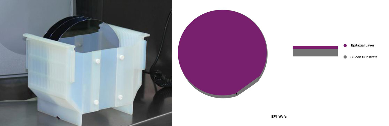
1:Epitaxy Wafer
Silicon Epitaxial Wafers are the core material used in manufacturing of a wide range of semiconductor devices with applications in consumer, industrial, military and space electronics.
| Diameter | 4" | 5" | 6" | 8" | |
| Device Layer | Dopant | Boron, Phos, Arsenic | |||
| Orientation | < 100 >, < 111 > | ||||
| Conductivity Type | P/P++, N/N++, N/N+, N/N+/N++, N/P/P, P/N/N+ | ||||
| Resistivity | 0.001-50 Ohm-cm | ||||
| Res. Uniformity | Standard < 6%, Maximum Capabilities < 2% | ||||
| Thickness(um) | 0.1-150 | ||||
| Thickness Uniformity | Standard < 3%, Maximum Capabilities < 1% | ||||
| Substrate | Orientation | < 100 >,< 111 > | |||
| Type/Dopant | P Type/Boron, N Type/Phos, N Type/As, N Type/Sb | ||||
| Thickness(um) | 300-725 | ||||
| Resistivity | 0.001-100 Ohm-cm | ||||
| Surface Finished | P/P, P/E | ||||
| Particle | < 50@.0.5um | ||||
Pluto provides a variety of production proven and industry standard Silicon Epitaxy process technologies for some of the most essential microelectronics applications:
Diodes
● Schottky diodes
● Ultra-fast diodes
● Zener diodes
● PIN diodes
● Transient Voltage Suppressors (TVS)
● and other
Transistors
● Power IGBT
● Power DMOS
● MOSFET
● Medium power
● Small-signal
● and other
Integrated Circuits
● Bipolar ICs
● EEPROM
● Amplifiers
● Microprocessors
● Microcontrollers
● RFID
● and other
To Integrated Circuit manufacturers PLUTO offers Silicon Epitaxial Deposition Services on substrates with buried ion-implanted or diffused layers.
Silicon substrates are either purchased from major global vendors or supplied by customer.
Epitaxy is a kind of interface between a thin film and a substrate. The term epitaxy (greek; "epi" "above" and "taxis" "in ordered manner") describes an ordered crystalline growth on a (single-) crystalline substrate. It involves the growth of crystals of one material on the crystal face of another (heteroepitaxy) or the same (homoepitaxy) material. The lattice structure and orientation or lattice symmetry of the thin film material is identical to that of the substrate on which it is deposited. Most importantly, if the substrate is a single crystal, then the thin film will also be a single crystal. Contrast with self-assembled monolayer and mesotaxy.
Some examples are molecular beam epitaxy, liquid phase epitaxy and vapor phase epitaxy. It has applications in nanotechnology and in the manufacture of semiconductor and photonic devices. Indeed, epitaxy is the only affordable method of high crystalline quality growth for many semiconductor materials, including the technologically important materials as SiGe, gallium nitride, gallium arsenide and indium phosphide, the latter used in devices for LEDs and telecommunications.
Epitaxial-growth means the crystal growth being conducted on crystal of substrate and disposed in accordance with foundation of substrate crystal phase.
Homoepitaxial means the growth of the same material as the substrate while heteroepitaxial means the growth of the different material from the substrate. Substrate wafer on which single crystal thin film deposited by epitaxial growth are generally called as epi wafer.
Silicon epi wafers are utilized for element of diode and transistor or substrate for IC such as bipolar type and MOS type.
Furthermore, multiple layer epi wafers and thick film epi wafers are often used for power device and contribute to smallness and energy-saving of various power-source products.
PLUTO can provide epitaxial grade wafers from our inventory or can grow custom epitaxial layers to meet your exact specifications.
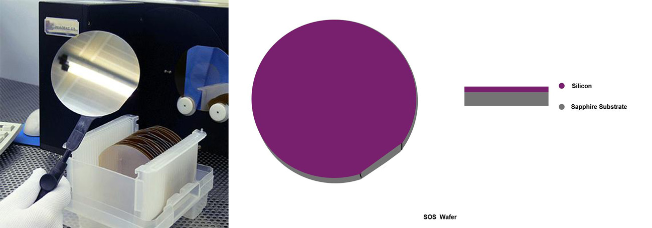
2: Silicon On Sapphire (SOS)
Sapphire (a-Al2O3) and spinel (MgO · Al2O3) are good insulators. Using them as substrates to epitaxial grow silicon to make integrated circuits can eliminate the interaction between components of integrated circuits, not only reduce leakage current and parasitic capacitance, enhance radiation resistance and reduce power consumption, but also improve integration and realize double-layer wiring. They are ideal materials for large-scale and super large-scale integrated circuits.
| Parameters range for Silicon on Sapphire (SOS) Epi Wafers | |
| Wafer diameter | 76 mm, 100 mm, 150 mm |
| Orientation | (1012) ± 1o (R-plane) |
| Substrate dopant | - |
| Epi-layer thickness, μm | 0,3 – 2,0 |
| Epi-layer dopant | Phosphorous, Boron |
| Epi-layer resistivity, Ohm.cm | - |
| n-type | according to spec. |
| p-type | 1,0 – 0,01 |
Heteroepitaxy of 5-6 silicon
With the development of large-scale and ultra large scale integrated circuits, epitaxy technology has been widely used. In addition to the homogeneous epitaxy of silicon on silicon substrate, the "SOS" epitaxy growth of silicon on sapphire and spinel substrate and the "SOI" heteroepitaxy growth of silicon on insulating substrate have also been developed. These two technologies and SiGe / I are briefly introduced in this section
5-6-1 SOS Technology
SOS is the abbreviation of "Silicon on sapphire" and "Silicon on spinel", i.e. epitaxial growth of silicon on sapphire or spinel substrate.
Sapphire (a-Al2O3) and spinel (MgO · Al2O3) are good insulators. Using them as substrates to epitaxial grow silicon to make integrated circuits can eliminate the interaction between components of integrated circuits, not only reduce leakage current and parasitic capacitance, enhance radiation resistance and reduce power consumption, but also improve integration and realize double-layer wiring. They are ideal materials for large-scale and super large-scale integrated circuits.
1. Selection of substrate materials
When choosing heteroepitaxial substrate materials, the first consideration is the compatibility between the epitaxial layer and substrate materials. Among them, crystal structure, melting point, vapor pressure, coefficient of thermal expansion and so on have a great influence on the quality of epitaxial layer. Secondly, the contamination of substrate on the epitaxial layer must be considered. At present, sapphire and spinel are the most suitable materials for silicon epitaxy. Table 5-4 lists the main physical properties of the two materials and silicon for comparison.
In terms of crystal structure, sapphire is hexagonal system, spinel is cubic system, and three silicon cells are consistent with two spinel cells. The mismatch of the two cells along (100 direction) is 0.7%. However, the spinel prepared by flame method is mostly aluminum rich. The lattice constant of this kind of spinel decreases with the increase of Al2O3 content, resulting in the increase of mismatch. On the other hand, the similar thermal expansion coefficient between the substrate and the epitaxial layer is one of the important factors for obtaining excellent heteroepitaxial layer. If the difference is large, the larger stress will be produced near the interface when the temperature changes, which will increase the defects of epitaxial layer, even warping, thus affecting the performance and thermal stability of materials and devices.
Considering lattice matching, thermal matching, reducing self doping and capacitance effect, spinel is a better substrate material than sapphire. However, the properties of silicon epitaxial layer on spinel are strongly dependent on the substrate components, which vary with different preparation methods and processing conditions. Therefore, although the silicon epitaxial layer on spinel substrate is superior to that on sapphire substrate, sapphire is widely used as silicon epitaxial substrate in current industrial production due to its poor reproducibility, high thermal conductivity and mature preparation process.
2. OS epitaxial growth
The equipment and basic process of OS epitaxial growth are the same as that of general silicon Homoepitaxy. The cutting, grinding, polishing and cleaning of substrate are basically the same, except that sapphire is harder than silicon, and the grinding and polishing time is longer.
In the process of SOS epitaxial growth, it is worth noting that the self doping effect is more serious, because under the condition of epitaxial growth, the substrate surface will react as follows:
Al2O3(s)+2HCl(g)+2H2(g)=2A1Cl(g)↑+3H20(g)
The chlorides of low valent aluminum are gaseous, which corrode the substrate and cause defects in the epitaxial layer. In addition, H2 and deposited silicon also corrode the substrate, and the reaction is as follows:
2H2(g)+al2O3(s)=al20(g)↑+2H2(g)
5Si(s)+2al2O3(s)=al20(g)↑+5Si(g)↑+2Al(s)
Before the substrate surface is completely covered by Si (at least the epitaxial layer is 10 ~ 20nm), all the above corrosion reactions are in progress. After the substrate surface is covered, these corrosion reactions will occur on the back of the substrate. Cause contamination such as a1o. In addition, due to the corrosion of the substrate surface, defects in the epitaxial layer will be increased, and even local polycrystalline growth will occur. Because the corrosion of SiCl4 to substrate is greater than that of SiH4, it is more advantageous to use SiH4 thermal decomposition method for SOS epitaxial growth.
In order to solve the contradiction between growth and corrosion, epitaxial growth methods such as double rate growth and two-step epitaxial growth can be used. The double rate growth method uses high growth rate (1 ~ 2 μ M / Mn) to quickly cover the substrate surface (growth 100 ~ 200nm). Then, it grows to the required thickness at a low growth rate (about 0.3m / min).
The two-step epitaxy is a comprehensive utilization of the advantages of SiH4 / H2 and sicl4h2 systems. In the first step, SiH4 / H2 system was used to rapidly cover the substrate surface, and then SiCl4 / 2 system was used to grow to the required thickness.
Due to the mechanical damage of the substrate surface and the corrosion between the growth components and the substrate, lattice mismatch, improper valence bond, strain effect and other factors, it is inevitable to introduce high-density dislocation, twin, intergranular boundary and other lattice defects in the epitaxial layer of SOS. These defects interact with heavy metal impurities such as Cu, Fe and form a series of deep energy levels in the forbidden band. In addition, there are some crystal defects in the epitaxial layer, such as A1 local precipitation and its oxide. They act as recombination, scattering and capture centers, which make the carrier concentration, mobility and minority carrier lifetime decrease. Therefore, the quality of SOS epitaxial layer can not catch up with that of homogeneous epitaxial layer, and the thinner the epitaxial layer, the worse the performance. In the future, it is an important subject for the development of SOS technology to improve the crystal integrity of SOS epitaxial layer, reduce self doping, make its performance close to the level of homogeneous silicon epitaxial layer and have good thermal stability.
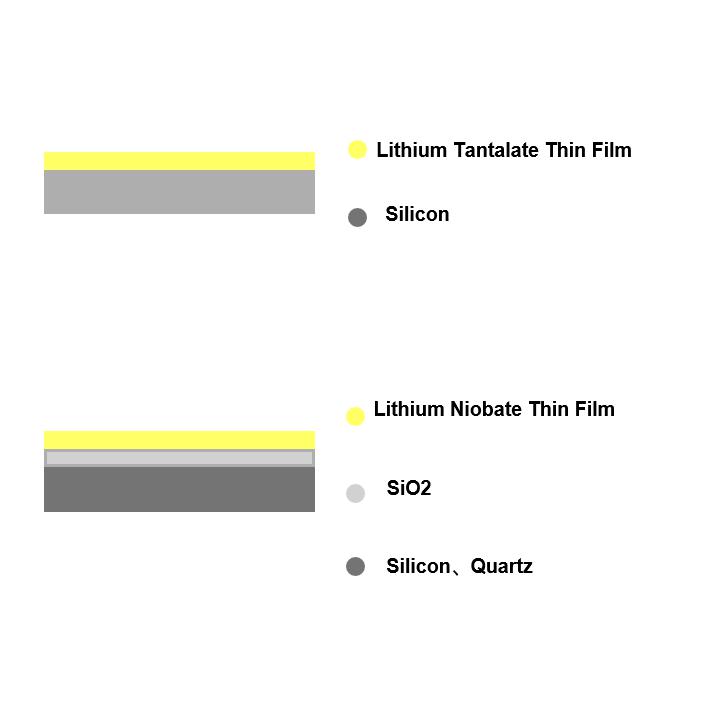
3: Lithium Tantalate and Lithium Niobate Thin Films
LT/Si bonded wafers are mainly used for temperature-compensated surface acoustic wave filters, which can better suppress temperature drift and facilitate processing.
4: InGaP、ALGaAs/GaAs and InP /InGaAs substrate epitaxy wafer
InGaAsP/GaAs heterostructured epitaxial wafer has good lattice matching, which is easy to realize microwave and optoelectronic devices and IC.
The lattice energy matching of InP /InGaAs heterostructured epitaxial sheets, in which InGaAs has a high electron mobility.
InGaP/GaAs heterostructured epitaxial sheets are not easily oxidized, have large valence band discontinuity and small valence discontinuity, and are the first choice for RF circuit design.
5: VCSEL epitaxy wafer
PLUTO offers VCSEL epitaxy at common wavelengths, such as 850nm, 940nm, and 1550nm. Structural customization is also available. Full epitaxial sheet or DIE available; Whether it's at the conceptual stage of product design, requiring an innovative upgrade to an existing product, or looking for an out-of-the-box solution. We can provide technical support for our customers' research and development projects and propose new methods and approaches to produce extensional structures that meet their requirements.
The 850 nm VCSEL epitaxial structure has an optical power of > 4mW, a low threshold current of 0.6 mA, and appropriate spectral characteristics for telecommunications and optical communication applications.
6: SiC epitaxy wafer
PLUTO's SiC epitaxy process provides customers with N type and P type doped semiconductor materials, which can produce 650V~3300V, 3300V~20000V unipolar and bipolar power devices, mainly including SBD, MOSFET, IGBT, JBS, etc. These power devices are widely used in new energy vehicles, photovoltaic energy storage, rail transit, smart grid, industrial power supplies and other fields.
We provide 4 inch, 6 inch epitaxial chip production (600V~3300V) power devices including SBD, JBS, PiN, MOSFET, JFET, BJT, GTO, IGBT, etc.
7: GaAs HEMT epitaxy
The pseudo high electron mobility transistor (PHEMT) based on GaAs epitaxial material is widely used in microwave and millimeter wave frequency bands because of its excellent performance such as high electron mobility, high current modulation efficiency and low loss.
8:GaAs/InP substrate SPAD epitaxy wafer
Photon avalanche diode (SPAD) is a photoelectric device that can detect single photons and is commonly used in low photon number detection applications such as quantum communication, single photon counting and imaging. GaAs (Gallium arsenide) and InP (indium phosphide) are two common semiconductor materials that are widely used to manufacture epitaxy sheets for SPAD devices.
9: InGaN/GaN LED epitaxy wafer
The basic principle of LED epitaxial wafer growth is that on a substrate heated to the appropriate temperature (mainly sapphire and, SiC, Si), the gaseous substance InGaAlP is controlled to the substrate surface to grow a specific single crystal film.
10: APD epitaxy wafer
GaAs base epitaxy wafer and InP base epitaxy wafer material are easy to grow and have high quantum efficiency and low dark current. Therefore, compared with ordinary radio and television diodes, avalanche diodes based on GaAs and InP epitaxial structures have the characteristics of high sensitivity, large current gain and fast frequency response.