


Wafer Foundry Services
We have electron beam direct writing, step lithography, laser direct writing, dry/wet etching, coating, cutting and other supporting processes, can provide a full range of micro and nano processing services from mold making, product process development, small batch to large-scale production.
Technological process:
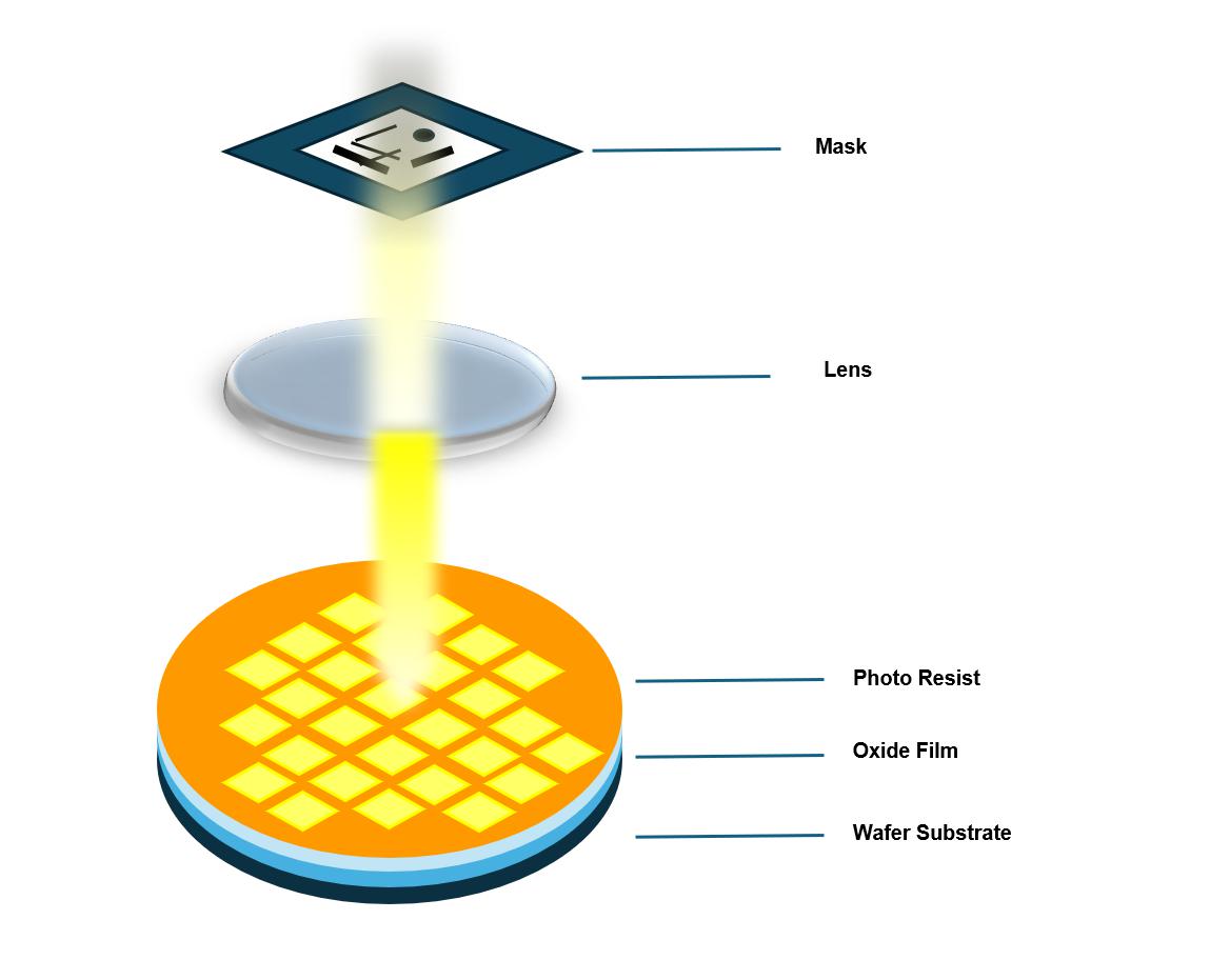
● Photoetching
We have double-sided UV lithography machine, DUV lithography machine, a variety of models of stepping lithography machine and matching glue development machine, in addition to the in separate child cleaning machine, HMDS oven and other kinds of lithography auxiliary equipment, can meet the 4 inch, 6 inch, 8 inch wafer lithography process.
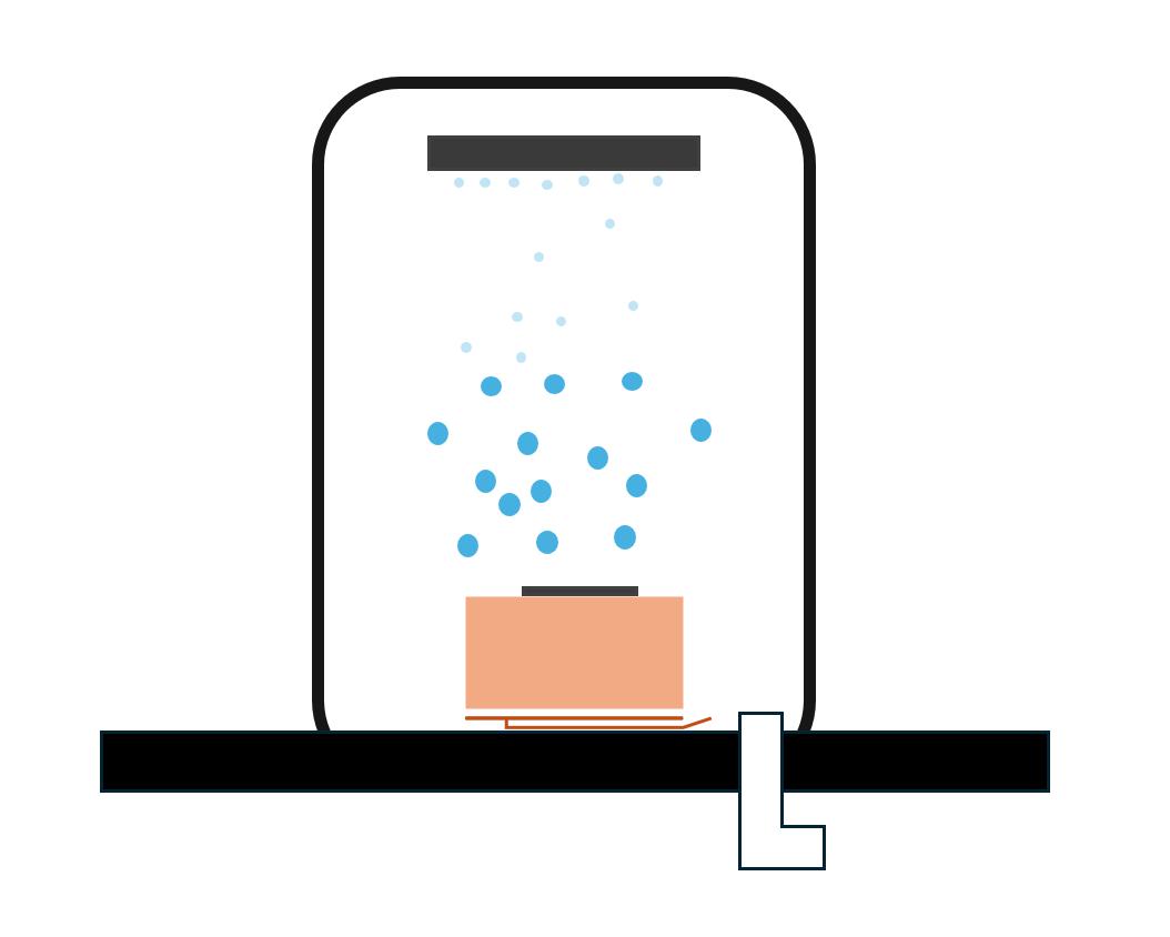
● Coating
We have plasma enhanced chemical Vapor deposition (PECVD), low pressure Chemical Vapor deposition (LPCVD), inductively coupled plasma chemical vapor deposition (ICPCVD), Atomic Layer deposition (ALD), multi-chamber magnetron sputtering, electron beam evaporation stations and other coating equipment, compatible with 8" and below wafers.
Materials available:
1.Ti, Al, Cu, Au, Cr, Pt, Ag, Mo, W, TiW, AuGe and other metal and alloy films
2.poly Si, a-Si, SiO2, SiNx, TEOS SiO2, ITO, Al2O3, TiO2, TiN, AlN
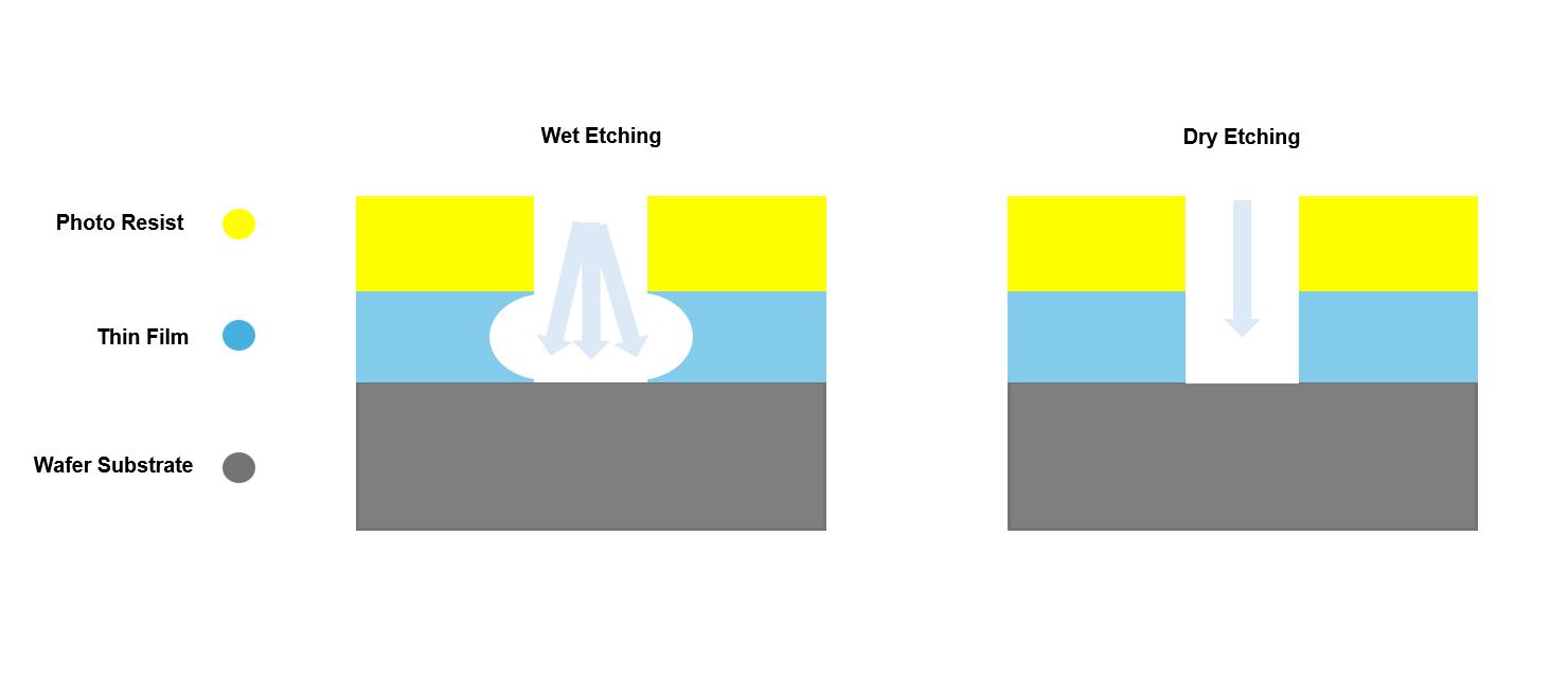
● Etching
We have reactive ion etching (RIE), inductively coupled plasma (ICP), ion beam etching (IBE), wet etching and other types of etching equipment, compatible with 8 inches and below etching process.
Etching material:
Si, SiO2, SiNx, a-Si, polysilicon, Au, Al, Cr, Ti, W, GaN, ITO, etc
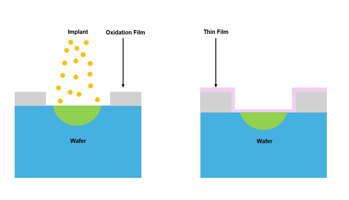
● Implant
We have a medium beam ion implanter equipment, compatible with 8 inches and below doping process, with a small doping depth (less than 1μm), doping is not limited by the equilibrium solid solubility and other advantages.
● Packaging
We have chemical mechanical polishing machine (CMP), bonding alignment machine, wafer temporary bonding machine, wafer permanent bonding machine, high pressure wafer bonding machine, silicon wafer cutting machine, compatible with 6 inch, 8 inch wafer bonding, cutting, thinning and other packaging equipment.
● Testing
We have field emission scanning electron microscope (FESEM), stress meter, ellipsometry, step meter, film thickness meter and other types of testing equipment.
